SLIS061D July 1998 – September 2015 TPIC6C595
PRODUCTION DATA.
- 1 Features
- 2 Applications
- 3 Description
- 4 Revision History
- 5 Pin Configuration and Functions
- 6 Specifications
- 7 Parameter Measurement Information
- 8 Detailed Description
- 9 Application and Implementation
- 10Power Supply Recommendations
- 11Layout
- 12Device and Documentation Support
- 13Mechanical, Packaging, and Orderable Information
Package Options
Refer to the PDF data sheet for device specific package drawings
Mechanical Data (Package|Pins)
- PW|16
- |
- N|16
- D|16
Thermal pad, mechanical data (Package|Pins)
Orderable Information
8 Detailed Description
8.1 Overview
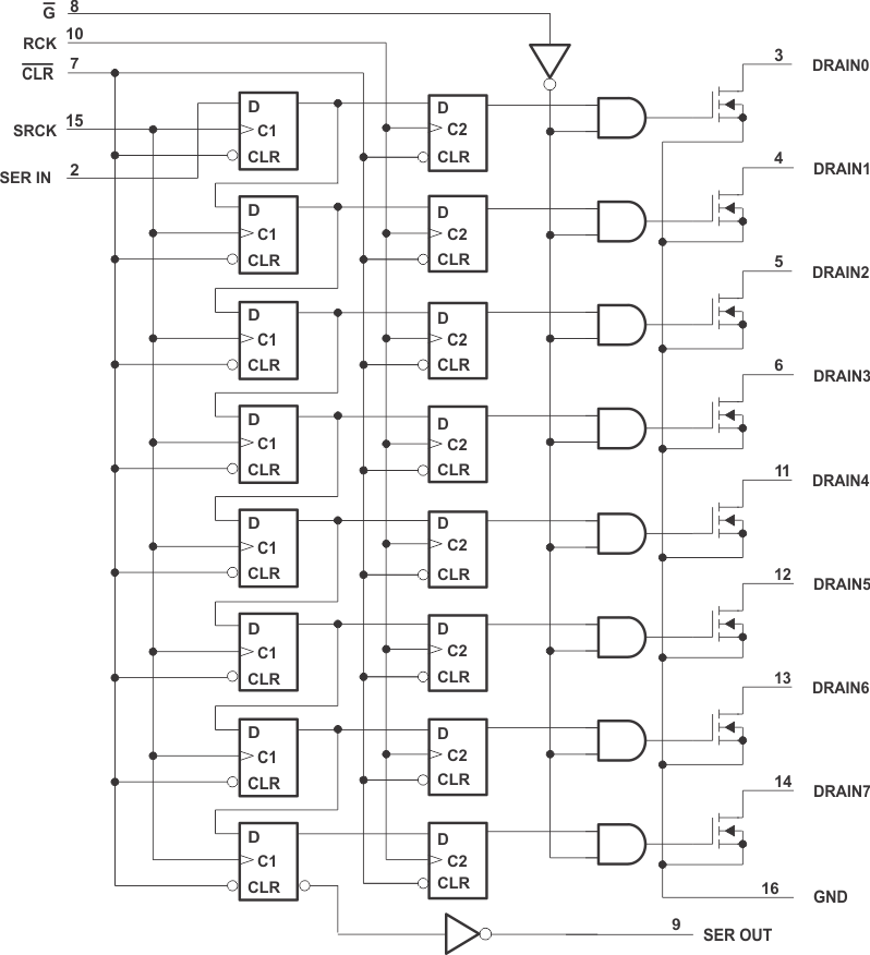
The TPIC6C595 is a monolithic, medium-voltage, low-current power 8-bit shift register designed to drive relatively moderate load power such as LEDs. The device contains a built-in voltage clamp on the outputs for inductive transient protection, so it can also drive relays, solenoids, and other low-current or medium-voltage loads.
8.2 Functional Block Diagram
 Figure 12. Logic Diagram (Positive Logic)
8.3 Feature Description
8.3.1 Serial-In Interface
This device contains an 8-bit serial-in, parallel-out shift register that feeds an 8-bit D-type storage register. Data transfers through both the shift and storage registers on the rising edge of the shift register clock (SRCK) and the register clock (RCK), respectively. The storage register transfers data to the output buffer when shift register clear (CLR) is high.
8.3.2 Clear Register
A logical low on (CLR) clears all registers in the device. TI suggests clearing the device during power up or initialization.
8.3.3 Output Control
Holding the output enable (G) high holds all data in the output buffers low, and all drain outputs are off. Holding (G) low makes data from the storage register transparent to the output buffers. When data in the output buffers is low, the DMOS transistor outputs are off. When data is high, the DMOS transistor outputs have sink-current capability. This pin can also be used for global PWM dimming.
8.3.4 Cascaded Application
The serial output (SER OUT) allows for cascading of the data from the shift register to additional devices. Connect the device (SEROUT) pin to the next device (SERIN) for daisy Chain.
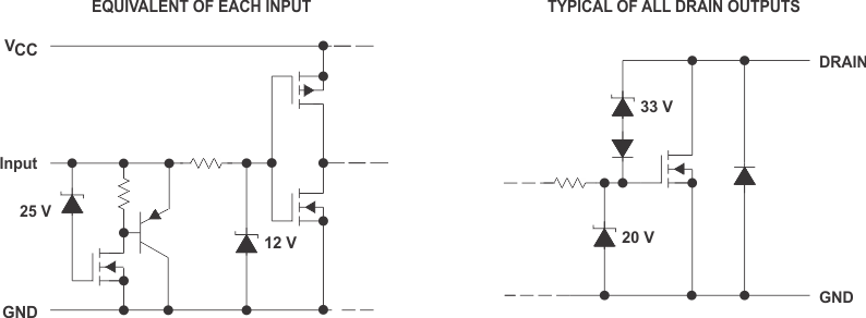
 Figure 13. Schematic of Inputs and Outputs
8.3.5 Current Limit Function
Outputs are low-side, open-drain DMOS transistors with output ratings of 33 V and 100-mA continuous sink current capability. Each output provides a 250-mA typical current limit at TC = 25°C. The current limit decreases as the junction temperature increases for additional device protection.
8.4 Device Functional Modes
8.4.1 Operation With V(VIN) < 4.5 V (Minimum V(VIN))
This device works normally during 4.5 V ≤ V(VIN) ≤ 5.5 V, when operation voltage is lower than 4.5 V. TI can't ensure the behavior of device, including communication interface and current capability.
8.4.2 Operating With 5.5 V < V(VIN) < 6 V
This device works normally during this voltage range, but reliability issues may occur while the device works for a long time in this voltage range.