SLIS093D March 2000 – March 2015 TPIC6C596
PRODUCTION DATA.
- 1 Features
- 2 Applications
- 3 Description
- 4 Revision History
- 5 Pin Configuration and Functions
- 6 Specifications
- 7 Parameter Measurement Information
- 8 Detailed Description
- 9 Application and Implementation
- 10Power Supply Recommendations
- 11Layout
- 12Device and Documentation Support
- 13Mechanical, Packaging, and Orderable Information
Package Options
Refer to the PDF data sheet for device specific package drawings
Mechanical Data (Package|Pins)
- PW|16
- N|16
- D|16
Thermal pad, mechanical data (Package|Pins)
Orderable Information
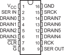
5 Pin Configuration and Functions
D, N, or PW Packages
16-Pin SOIC, PDIP, and TSSOP
Top View

Pin Functions
| PIN | I/O | DESCRIPTION | |
|---|---|---|---|
| NAME | NO. | ||
| CLR | 7 | I | Shift register clear, active-low |
| DRAIN0 | 3 | O | Open-drain output |
| DRAIN1 | 4 | O | Open-drain output |
| DRAIN2 | 5 | O | Open-drain output |
| DRAIN3 | 6 | O | Open-drain output |
| DRAIN4 | 11 | O | Open-drain output |
| DRAIN5 | 12 | O | Open-drain output |
| DRAIN6 | 13 | O | Open-drain output |
| DRAIN7 | 14 | O | Open-drain output |
| G | 8 | I | Output enable, active-low |
| GND | 16 | — | Power ground |
| RCK | 10 | I | Register clock |
| SER IN | 2 | I | Serial data input |
| SER OUT | 9 | O | Serial data output |
| SRCK | 15 | I | Shift register clock |
| VCC | 1 | I | Power supply |