SLIS135E December 2010 – February 2017
PRODUCTION DATA.
- 1 Features
- 2 Applications
- 3 Description
- 4 Revision History
- 5 Pin Configuration and Functions
- 6 Specifications
- 7 Detailed Description
- 8 Application and Implementation
- 9 Power Supply Recommendations
- 10Layout
- 11Device and Documentation Support
- 12Mechanical, Packaging, and Orderable Information
Package Options
Mechanical Data (Package|Pins)
- RTE|16
Thermal pad, mechanical data (Package|Pins)
- RTE|16
Orderable Information
6 Specifications
6.1 Absolute Maximum Ratings
over operating free-air temperature range (unless otherwise noted)(1) (2) (3)| MIN | MAX | UNIT | |||
|---|---|---|---|---|---|
| Supply voltage | VDD to GND | –0.3 | 7 | V | |
| All other pins to GND | –0.3 | VDD + 0.3 | V | ||
| IL
IW IH |
Pulse current | ±20 | mA | ||
| Continuous current | TPL0202-10 | ±2 | mA | ||
| Tstg | Storage temperature | –65 | 150 | °C | |
(1) Stresses beyond those listed under Absolute Maximum Ratings may cause permanent damage to the device. These are stress ratings only, which do not imply functional operation of the device at these or any other conditions beyond those indicated under Recommended Operating Conditions. Exposure to absolute-maximum-rated conditions for extended periods may affect device reliability.
(2) Follows the algebraic convention, whereby the most negative value is a minimum and the most positive value is a maximum.
(3) All voltages are with respect to ground, unless otherwise specified.
6.2 ESD Ratings
| VALUE | UNIT | |||
|---|---|---|---|---|
| V(ESD) | Electrostatic discharge | Human-body model (HBM), per ANSI/ESDA/JEDEC JS-001(1) | ±2500 | V |
| Charged-device model (CDM), per JEDEC specification JESD22-C101(2) | ±1000 | |||
(1) JEDEC document JEP155 states that 500-V HBM allows safe manufacturing with a standard ESD control process.
(2) JEDEC document JEP157 states that 250-V CDM allows safe manufacturing with a standard ESD control process.
6.3 Recommended Operating Conditions
over operating free-air temperature range (unless otherwise noted)| MIN | MAX | UNIT | |||
|---|---|---|---|---|---|
| VDD,GND | 2.7 | 5.5 | V | ||
| VH, VL, VW | Terminal voltage range | 0 | VDD | V | |
| VIH | Voltage input high (SCLK, DIN, CS) | VDD = 3.6 V to 5.5 V | 2.4 | 5.5 | V |
| VDD = 2.7 V to 3.6 V | 0.7 × VDD | 5.5 | |||
| VIL | Voltage input low (SCLK, DIN, CS) | 0 | 0.8 | V | |
| IW | Wiper current | ±2 | mA | ||
| TA | Free-air ambient temperature | –40 | 105 | °C | |
6.4 Thermal Information
| THERMAL METRIC(1) | TPL0202 | UNIT | |
|---|---|---|---|
| RTE (WQFN) | |||
| 16 PINS | |||
| RθJA | Junction-to-ambient thermal resistance | 73.2 | °C/W |
| RθJC(top) | Junction-to-case (top) thermal resistance | 33.4 | °C/W |
| RθJB | Junction-to-board thermal resistance | 34.9 | °C/W |
| ψJT | Junction-to-top characterization parameter | 0.3 | °C/W |
| ψJB | Junction-to-board characterization parameter | 34.9 | °C/W |
| RθJC(bot) | Junction-to-case (bottom) thermal resistance | 23.5 | °C/W |
(1) For more information about traditional and new thermal metrics, see the Semiconductor and IC Package Thermal Metrics application report.
6.5 Electrical Characteristics
VDD = 2.7 to 5.5 V, TA= –40°C to +105°C (unless otherwise noted). Typical values are at VDD= 5 V, TA= 25°C (unless otherwise noted).| PARAMETER | TEST CONDITIONS | MIN | TYP | MAX | UNIT | |||
|---|---|---|---|---|---|---|---|---|
| RTOT | End-to-end resistance (between H and L terminals) |
VL = VDD / 2, IHL = 100 µA, Input code = 0x80, Measure VHL | 8 | 10 | 12 | kΩ | ||
| RH | High terminal resistance | VL = VDD / 2, IHL = 100 µA, Input code = 0xFF, Measure VHW | 100 | 200 | Ω | |||
| RL | Low terminal resistance | VL = VDD / 2, IHL = 100 µA, Input code = 0x00, Measure VWL | 60 | 200 | Ω | |||
| RW | Wiper resistance | VL = VDD / 2, IWL = 100 µA, Input code = 0x00, Measure VHW | 25 | 100 | Ω | |||
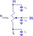
| CH, CL (14) (15) | Terminal capacitance | 22 | pF | |||||
| CW (14) (15) | Wiper capacitance | 18 | pF | |||||
| ILKG | Terminal leakage current | VH = VSS to VDD, VL = Floating OR VL = VSS to VDD, VH = Floating |
0.1 | 1 | µA | |||
| TCR | Resistance temperature coefficient | Input code = 0x80h | 132 | ppm/°C | ||||
| RTOT,MATCH | Channel-to-channel resistance match | 0.1% | ||||||
| VOLTAGE DIVIDER MODE | ||||||||
| INL(1) (3) | Integral non-linearity | –1 | 1 | LSB | ||||
| DNL(1) (4) | Differential non-linearity | –0.5 | 0.5 | LSB | ||||
| ZSERROR (2) (5) | Zero-scale error | 0 | 2 | 5 | LSB | |||
| FSERROR (2) (6) | Full-scale error | –5 | –2 | 0 | LSB | |||
| VMATCH (2) (7) | Channel-to-channel matching | Wiper at the same tap position, same voltage all H and the same voltage at all L terminals | –2 | 2 | LSB | |||
| TCV | Ratiometric temperature coefficient | Wiper set at midscale | 12 | ppm/°C | ||||
| BW | Bandwidth | Wiper set at midscale CLOAD = 10 pF VL = VDD / 2, Signal applied to H; measurement at W |
2000 | kHz | ||||
| two | Register write to output time | Time from CS rising edge to 90% of expected value | 2 | µs | ||||
| THD+N | Total harmonic distortion + noise | VHL = 1 VRMS at 1 kHz, VL = VDD / 2, Measurement at W |
0.03% | |||||
| XTALK | Crosstalk | fH_A = 1 kHz, VL_A = VL_B = VDD / 2, VH_B = Floating Measurement at W_A and W_B |
–94 | dB | ||||
| RHEOSTAT MODE (Measurements between W and L with H not connected, or between W and H with L not connected) | ||||||||
| RINL (8) (10) | Integral non-linearity | –1.5 | 1.5 | LSB | ||||
| RDNL(8) (11) | Differential non-linearity | –0.5 | 0.5 | LSB | ||||
| ROFFSET (9) (12) | Offset | 0 | 2.5 | 7 | LSB | |||
| RMATCH (9) (13) | Channel-to-channel matching | –2 | 2 | LSB | ||||
(1) LSB = (VMEAS[code 255] – VMEAS[code 0]) / 255
(2) IDEAL_LSB = (VH – VL) / 256
(3) INL = ((VMEAS[code x] – VMEAS[code 0]) / LSB) – [code x]
(4) DNL = ((VMEAS[code x] – VMEAS[code x-1]) / LSB) – 1
(5) ZSERROR = VMEAS[code 0] / IDEAL_LSB
(6) FSERROR = [(VMEAS[code 255] – (VH – VL)) / IDEAL_LSB] + 1
(7) VMATCH = (VMEAS_A[code x] – VMEAS_B[code x]) / IDEAL_LSB
(8) RLSB = (RMEAS[code 255] – RMEAS[code 0]) / 255
(9) IDEAL_RLSB = RTOT / 256
(10) RINL =((RMEAS[code x] – RMEAS[code 0]) / RLSB) - [code x]
(11) RDNL = ((RMEAS[code x] – RMEAS[code x-1]) / RLSB ) – 1
(12) ROFFSET = RMEAS[code 0] / IDEAL_RLSB
(13) RMATCH = (RMEAS_A[code x] – RMEAS_B[code x]) / IDEAL_RLSB
(14) Terminal and wiper capacitance extracted from self admittance of three-port network measurement


(15) Digital potentiometer macromodel

6.6 Operating Characteristics
VDD = 2.7 V to 5.5 V, VH= VDD, VL= GND, TA= –40°C to +105°C (unless otherwise noted). Typical values are at VDD= 5 V, TA= 25°C (unless otherwise noted).6.7 SPI Timing Requirements
VDD = 2.7 V to 5.5 V, VH= VDD, VL= GND, TA= –40°C to +105°C (unless otherwise noted)6.8 Typical Characteristics
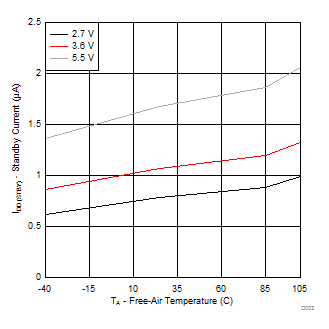 Figure 1. Standby Current vs Temperature
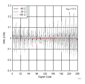 Figure 3. Voltage Divider Mode DNL vs Temperature
 (VDD = 5 V)
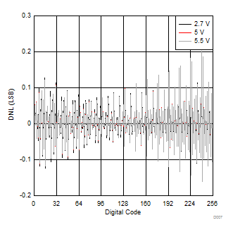 Figure 5. Voltage Divider Mode DNL vs Supply Voltage (25°C)
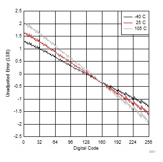 Figure 7. Voltage Divider Mode Unadjusted Error (VDD = 5V)
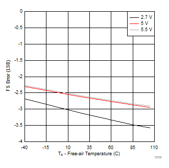 Figure 9. Voltage Divider Mode FS Error vs Temperature
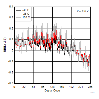 Figure 11. Rheostat Mode RINL vs Temperature (VDD = 5 V)
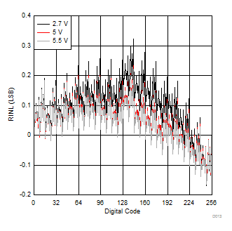 Figure 13. Rheostat Mode RINL vs Supply Voltage (25°C)
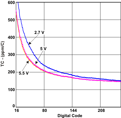 Figure 15. Rheostat Mode TC vs Digital Code
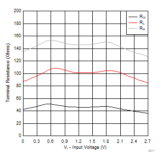 Figure 17. Wiper and Terminal Resistance (VDD = 2.7 V)
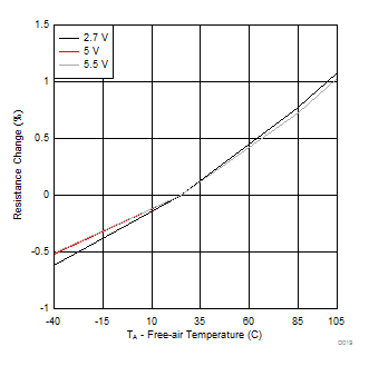 Figure 19. End-End Resistance Change vs Temperature
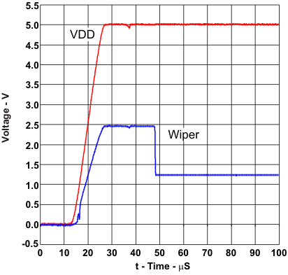 Figure 21. tPOR (Power-Up Response Time) Non-Volatile Memory = 40h
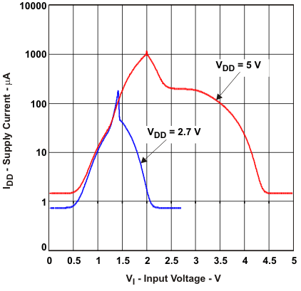 Figure 2. Supply Current vs Digital Input Voltage
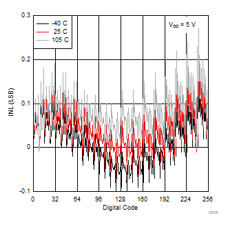 Figure 4. Voltage Divider Mode INL vs Temperature
 (VDD = 5 V)
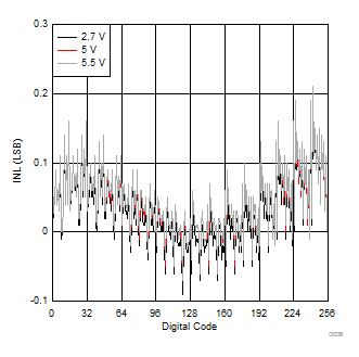 Figure 6. Voltage Divider Mode INL vs Supply Voltage (25°C)
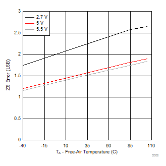 Figure 8. Voltage Divider Mode ZS Error vs Temperature
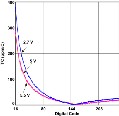 Figure 10. Voltage Divider Mode vs Digital Code
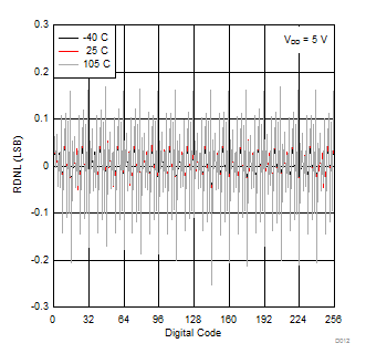 Figure 12. Rheostat Mode RDNL vs Temperature (VDD = 5 V)
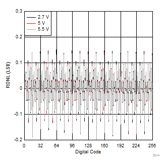 Figure 14. Rheostat Mode RDNL vs Supply Voltage (25°C)
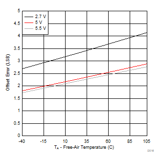 Figure 16. Rheostat Mode Offset Error vs Temperature
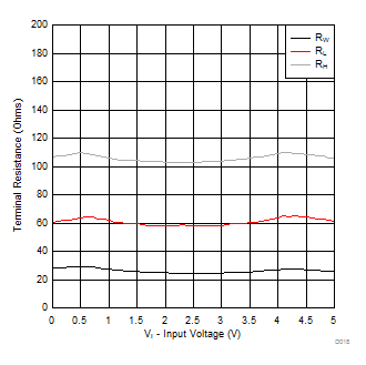 Figure 18. Wiper and Terminal Resistance (VDD = 5 V)
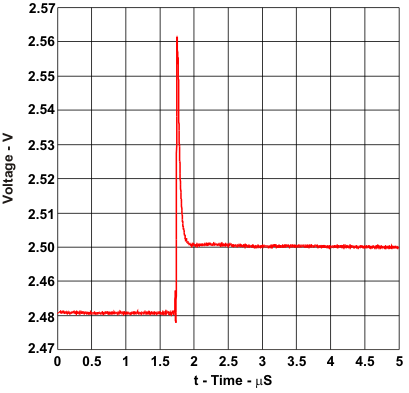 Figure 20. Midscale Wiper Glitch (Code 7fh to 80h) VDD = 5 V, VH = VDD, VL = GND, Cload = 10 pF