SNAS651A January   2015  – September 2018 TPL5010

PRODUCTION DATA.  

  1. Features
  2. Applications
  3. Description
    1.     Device Images
      1.      Simplified Application Schematic
  4. Revision History
  5. Device Comparison Table
  6. Pin Configuration and Functions
    1.     Pin Functions
  7. Specifications
    1. 7.1 Absolute Maximum Ratings
    2. 7.2 ESD Ratings
    3. 7.3 Recommended Operating Ratings
    4. 7.4 Thermal Information
    5. 7.5 Electrical Characteristics
    6. 7.6 Timing Requirements
    7. 7.7 Typical Characteristics
  8. Detailed Description
    1. 8.1 Overview
    2. 8.2 Functional Block Diagram
    3. 8.3 Feature Description
      1. 8.3.1 WAKE
      2. 8.3.2 DONE
      3. 8.3.3 RSTn
    4. 8.4 Device Functional Modes
      1. 8.4.1 Start-Up
      2. 8.4.2 Normal Operating Mode
    5. 8.5 Programming
      1. 8.5.1 Configuring the WAKE Interval With the DELAY/M_RST Pin
      2. 8.5.2 Manual Reset
        1. 8.5.2.1 DELAY/M_RST
        2. 8.5.2.2 Circuitry
      3. 8.5.3 Timer Interval Selection Using External Resistance
      4. 8.5.4 Quantization Error
      5. 8.5.5 Error Due to Real External Resistance
  9. Application and Implementation
    1. 9.1 Application Information
    2. 9.2 Typical Application
      1. 9.2.1 Design Requirements
      2. 9.2.2 Detailed Design Procedure
      3. 9.2.3 Application Curve
  10. 10Power Supply Recommendations
  11. 11Layout
    1. 11.1 Layout Guidelines
    2. 11.2 Layout Example
  12. 12Device and Documentation Support
    1. 12.1 Receiving Notification of Documentation Updates
    2. 12.2 Community Resources
    3. 12.3 Trademarks
    4. 12.4 Electrostatic Discharge Caution
    5. 12.5 Glossary
  13. 13Mechanical, Packaging, and Orderable Information

Package Options

Mechanical Data (Package|Pins)
Thermal pad, mechanical data (Package|Pins)
Orderable Information

Typical Characteristics

TPL5010 D018_SNAS651.gif
Figure 2. IDD vs. VDD
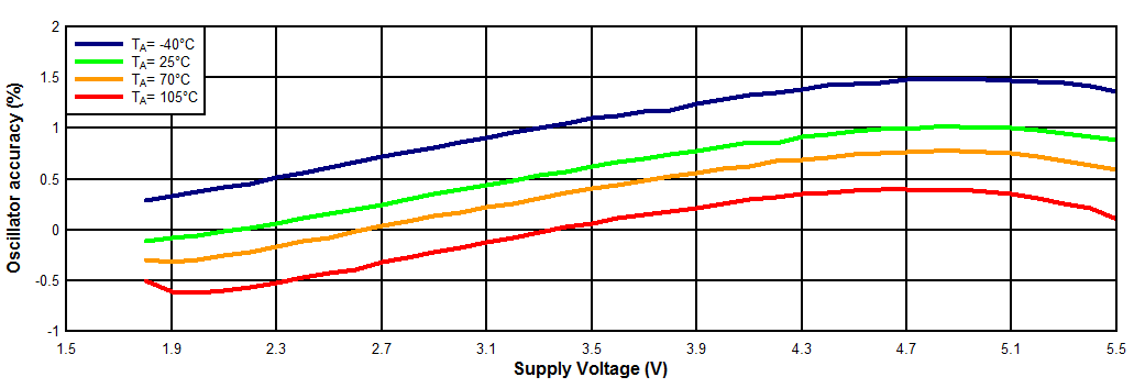
TPL5010 D021_SNAS651.gif
Figure 4. Oscillator Accuracy vs. VDD
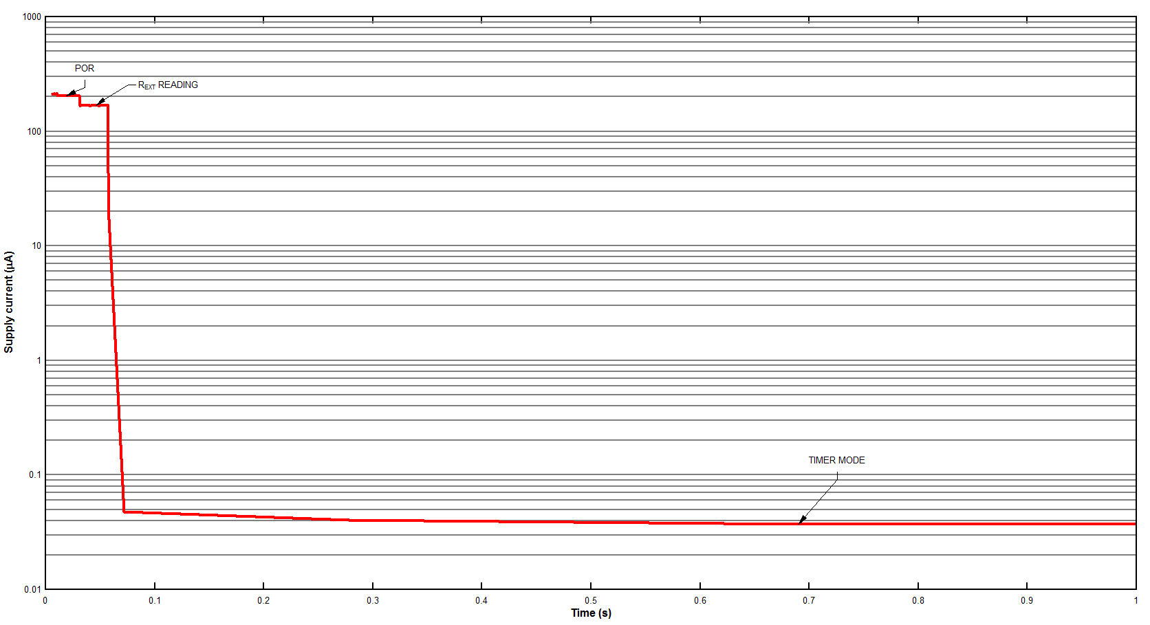
TPL5010 D031_SNAS650.gif
Figure 6. IDD vs. Time
TPL5010 D017_SNAS651.gif
Figure 3. IDD vs. Temperature
TPL5010 D019_SNAS651.gif
Figure 5. Oscillator Accuracy vs. Temperature
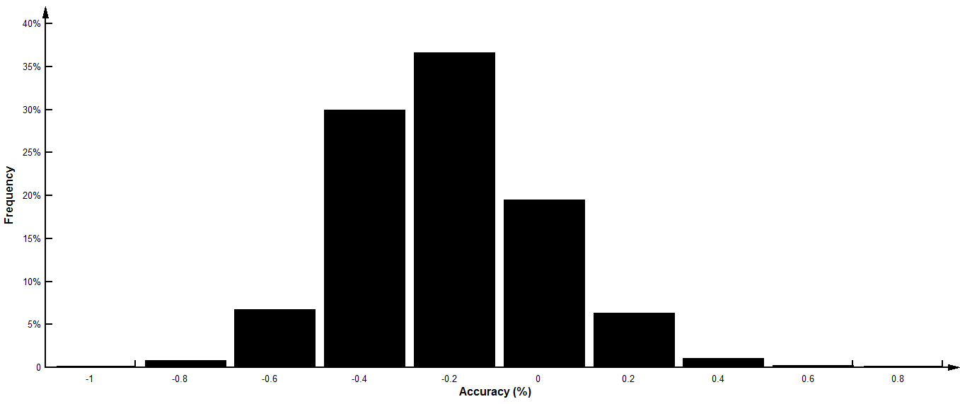
TPL5010 D022_SNAS651.gif
number of observations >20000 1s < tIP ≤ 7200s
Figure 7. Time Interval Setting Accuracy