SNAS681A February 2017 – September 2021 TPL5110-Q1
PRODUCTION DATA
- 1 Features
- 2 Applications
- 3 Description
- 4 Revision History
- 5 Pin Configuration and Functions
- 6 Specifications
- 7 Detailed Description
- 8 Application and Implementation
- 9 Power Supply Recommendations
- 10Layout
- 11Device and Documentation Support
- 12Mechanical, Packaging, and Orderable Information
Package Options
Mechanical Data (Package|Pins)
- DDC|6
Thermal pad, mechanical data (Package|Pins)
Orderable Information
7.5.2 Manual MOSFET Power ON Applied to the DELAY/M_DRV Pin
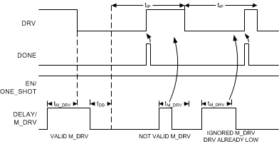
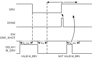
If VDD is connected to the DELAY/M_DRV pin, the TPL5110-Q1 recognizes this as a manual MOSFET Power ON condition. In this case the time interval is not set. If the manual MOSFET Power ON is asserted during the POR or during the reading procedure, the reading procedure is aborted and is re-started as soon as the manual MOSFET Power ON switch is released. A pulse on the DELAY/M_DRV pin is recognized as a valid manual MOSFET Power ON only if it lasts at least 20ms (observation time is 30ms). The manual MOSFET Power ON may be implemented using a switch (momentary mechanical action).
If the DRV is already LOW (MOSFET ON) the manual MOSFET Power ON is ignored.
 Figure 7-4 Manual MOSFET Power ON in Timer Mode
 Figure 7-5 Manual MOSFET Power ON in One-Shot
Mode