SNAS659B
June 2015 – September 2018
TPL5111
PRODUCTION DATA.
1
Features
2
Applications
3
Description
Device Images
Simplified Application Schematic
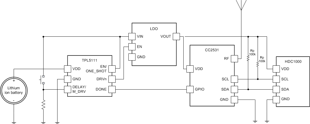
4
Revision History
5
Pin Configuration and Functions
Pin Functions
6
Specifications
6.1
Absolute Maximum Ratings
6.2
ESD Ratings
6.3
Recommended Operating Ratings
6.4
Thermal Information
6.5
Electrical Characteristics
6.6
Timing Requirements
6.7
Typical Characteristics
7
Detailed Description
7.1
Overview
7.2
Functional Block Diagram
7.3
Feature Description
7.3.1
DRVn
7.3.2
DONE
7.4
Device Functional Modes
7.4.1
Start-Up
7.4.2
Timer Mode
7.4.3
One-Shot Mode
7.5
Programming
7.5.1
Configuring the Time Interval With the DELAY/M_DRV Pin
7.5.2
Manual Power ON Applied to the DELAY/M_DRV Pin
7.5.2.1
DELAY/M_DRV
7.5.2.2
Circuitry
7.5.3
Selection of the External Resistance
7.5.4
Quantization Error
7.5.5
Error Due to Real External Resistance
8
Application and Implementation
8.1
Application Information
8.2
Typical Application
8.2.1
Design Requirements
8.2.2
Detailed Design Procedure
8.2.3
Application Curve
9
Power Supply Recommendations
10
Layout
10.1
Layout Guidelines
10.2
Layout Example
11
Device and Documentation Support
11.1
Receiving Notification of Documentation Updates
11.2
Community Resources
11.3
Trademarks
11.4
Electrostatic Discharge Caution
11.5
Glossary
12
Mechanical, Packaging, and Orderable Information
Package Options
Mechanical Data (Package|Pins)
DDC|6
MPDS124I
Thermal pad, mechanical data (Package|Pins)
Orderable Information
snas659b_oa
snas659b_pm
Device Images
Simplified Application Schematic