SCPS301 September 2024 TPLD801-Q1
ADVANCE INFORMATION
- 1
- 1Features
- 2Applications
- 3Description
- 4Pin Configuration and Functions
- 5Specifications
- 6Parameter Measurement Information
-
7Detailed Description
- 7.1 Overview
- 7.2 Functional Block Diagram
- 7.3 Feature Description
- 7.4 Device Functional Modes
- 7.5 Programming
- 8Revision History
- 9Mechanical, Packaging, and Orderable Information
Package Options
Mechanical Data (Package|Pins)
- DRL|8
Thermal pad, mechanical data (Package|Pins)
Orderable Information
6 Parameter Measurement Information
Phase relationships between waveforms were chosen arbitrarily. All input pulses are supplied by generators having the following characteristics: PRR ≤ 1MHz, ZO = 50Ω, tt < 2.5 ns.
For clock inputs, fmax is measured when the input duty cycle is 50%.
The outputs are measured one at a time with one input transition per measurement.
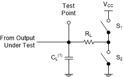
(1) CL includes probe
and test-fixture capacitance.
Figure 6-1 Load Circuit for 3-State
Outputs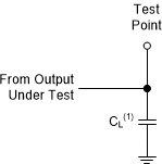
(1) CL includes probe
and test-fixture capacitance.
Figure 6-3 Load Circuit for Push-Pull
Outputs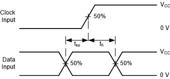 Figure 6-5 Voltage Waveforms, Setup
and Hold Times
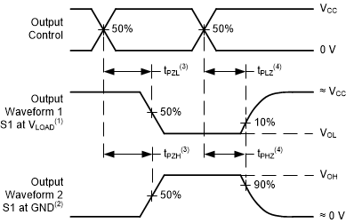 Figure 6-7 Voltage Waveforms
Propagation Delays
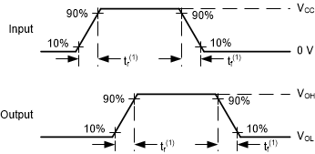
(1) The greater between
tr and tf is the same as tt.
Figure 6-9 Voltage Waveforms, Input
and Output Transition Times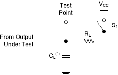
(1)
CL includes probe and test-fixture capacitance.
Figure 6-2 Load Circuit for
Open-Drain Outputs Figure 6-4 Voltage Waveforms, Pulse
Duration
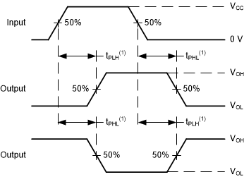
(1) The
greater between tPLH and tPHL is the same as
tpd.
Figure 6-6 Voltage Waveforms
Propagation Delays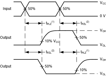
(1) The greater between
tPLZ and tPZL is the same as
tpd.
Figure 6-8 Voltage Waveforms
Propagation Delays