SLUSFA1 September 2024 TPS1214-Q1
ADVANCE INFORMATION
- 1
- 1 Features
- 2 Applications
- 3 Description
- 4 Device Comparison
- 5 Pin Configuration and Functions
- 6 Specifications
- 7 Parameter Measurement Information
-
8 Detailed Description
- 8.1 Overview
- 8.2 Functional Block Diagram
- 8.3
Feature Description
- 8.3.1 Charge Pump and Gate Driver Output (VS, GATE, BST, SRC)
- 8.3.2 Capacitive Load Driving
- 8.3.3 Overcurrent and Short-Circuit Protection
- 8.3.4 Analog Current Monitor Output (IMON)
- 8.3.5 NTC based Temperature Sensing (TMP) and Analog Monitor Output (ITMPO)
- 8.3.6 Fault Indication and Diagnosis (FLT, SCP_TEST)
- 8.3.7 Reverse Polarity Protection
- 8.3.8 Undervoltage Protection (UVLO)
- 8.4 Device Functional Modes
- 9 Application and Implementation
- 10Device and Documentation Support
- 11Revision History
- 12Mechanical, Packaging, and Orderable Information
Package Options
Mechanical Data (Package|Pins)
- RGE|23
Thermal pad, mechanical data (Package|Pins)
Orderable Information
12.1 Tape and Reel Information
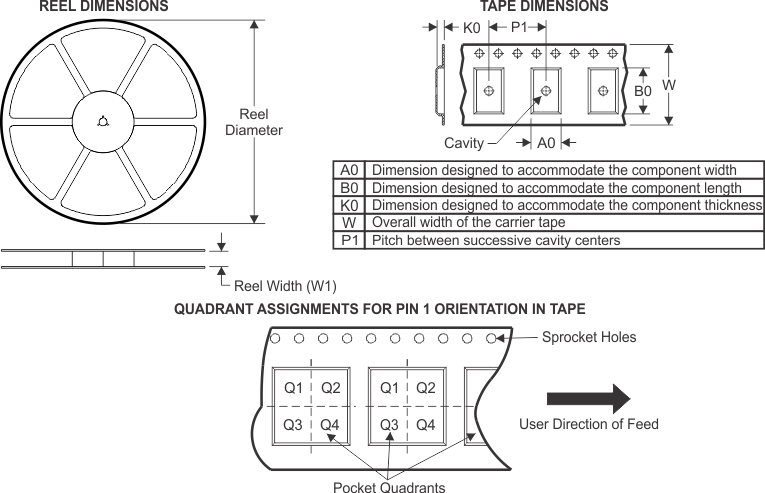
| Device | Package Type | Package Drawing | Pins | SPQ | Reel Diameter (mm) | Reel Width W1 (mm) | A0 (mm) | B0 (mm) | K0 (mm) | P1 (mm) | W (mm) | Pin1 Quadrant |
|---|---|---|---|---|---|---|---|---|---|---|---|---|
|
PTPS12140QRGERQ1 |
VQFN |
RGE |
23 | 3000 | 330.0 |
12.4 | 4.25 |
4.25 |
1.15 |
8.0 |
12.0 |
Q2 |
| PTPS12141QRGERQ1 | VQFN | RGE |
23 | 3000 | 330.0 | 12.4 | 4.25 | 4.25 | 1.15 | 8.0 | 12.0 | Q2 |
| PTPS12142QRGERQ1 | VQFN | RGE |
23 | 3000 | 330.0 | 12.4 | 4.25 | 4.25 | 1.15 | 8.0 | 12.0 | Q2 |
| PTPS12143QRGERQ1 | VQFN | RGE |
23 | 3000 | 330.0 | 12.4 | 4.25 | 4.25 | 1.15 | 8.0 | 12.0 | Q2 |
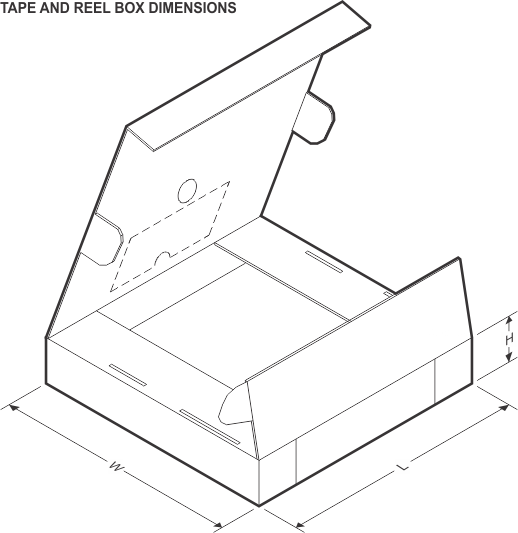
| Device | Package Type | Package Drawing | Pins | SPQ | Length (mm) | Width (mm) | Height (mm) |
|---|---|---|---|---|---|---|---|
| PTPS12140QRGERQ1 |
VQFN |
RGE |
23 |
3000 |
367.0 |
367.0 |
35.0 |
| PTPS12141QRGERQ1 | VQFN | RGE | 23 |
3000 |
367.0 | 367.0 | 35.0 |
| PTPS12142QRGERQ1 | VQFN | RGE |
23 |
3000 |
367.0 | 367.0 | 35.0 |
| PTPS12143QRGERQ1 | VQFN | RGE |
23 |
3000 | 367.0 | 367.0 | 35.0 |