SLVSGF4B june 2022 – may 2023 TPS1641
PRODUCTION DATA
- 1 Features
- 2 Applications
- 3 Description
- 4 Revision History
- 5 Device Comparison Table
- 6 Pin Configuration and Functions
- 7 Specifications
-
8 Detailed Description
- 8.1 Overview
- 8.2 Functional Block Diagram
- 8.3
Feature Description
- 8.3.1 Enable and Shutdown Input (EN/SHDN)
- 8.3.2 Overvoltage Protection (OVP)
- 8.3.3 Output Slew Rate and Inrush Current Control (dVdt)
- 8.3.4 Active Current Limiting (ILIM) With the TPS16412, TPS16413, TPS16416, and TPS16417
- 8.3.5 Active Power Limiting (PLIM) With the TPS16410, TPS16411, TPS16414, and TPS16415
- 8.3.6 Overcurrent Protection (IOCP) and Blanking Time (IDLY or PDLY) for Transient Loads
- 8.3.7 Fast-Trip and Short-Circuit Protection
- 8.3.8 Analog Load Current Monitor (IMON) on the IOCP Pin
- 8.3.9 IN to OUT Short Detection (TPS16410, TPS16411, TPS16412, and TPS16413)
- 8.3.10 Thermal Shutdown and Overtemperature Protection
- 8.3.11 Fault Response and Indication (FLT)
- 8.4 Device Functional Modes
- 9 Application and Implementation
- 10Device and Documentation Support
- 11Mechanical, Packaging, and Orderable Information
Package Options
Mechanical Data (Package|Pins)
- DRC|10
Thermal pad, mechanical data (Package|Pins)
- DRC|10
Orderable Information
8.3.1 Enable and Shutdown Input (EN/SHDN)
The TPS1641x devices include a enable and shutdown input. Keeping EN/SHDN low for a duration more than tLow_SHDN brings the device into low power shutdown mode, internal blocks of device are turned off, and the quiescent current of the device is reduced to IQSD from Vcc supply.
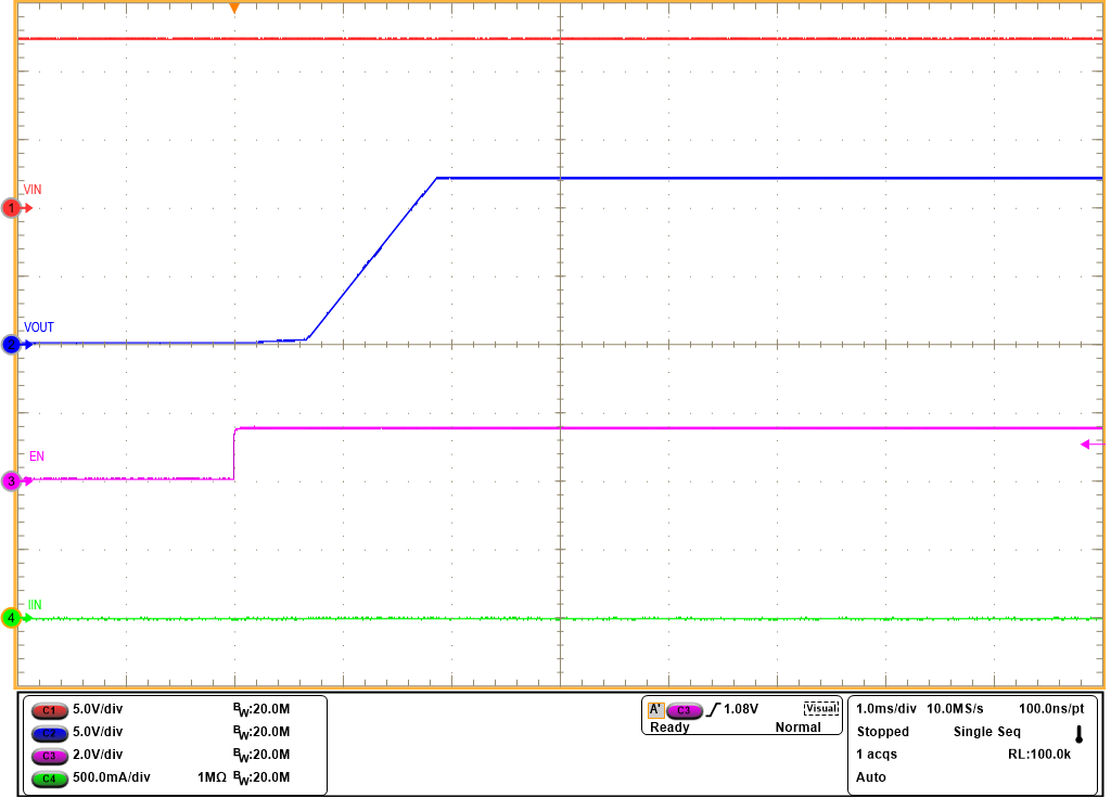
While keeping EN/SHDN low for a duration less than tLow_SHDN, the device turns off the internal FET only and FET can be turned back on quickly. The device turns off the internal FET with a delay of tEN_OFF_dly as the enable pin is brought low. The internal FET can be enabled quickly with a delay of tEN_ON_dly when the device is not in shutdown. See the Section 7.5 for VENR and VENF thresholds and the Section 7.6 for tLow_SHDN, tEN_OFF_dly, and tEN_ON_dly timings. A PWM signal with low period less than tLow_SHDN can be provided on EN/SHDN pin of the device for fast turn-on and turn-off of internal FET. Figure 8-1 illustrates the EN/SHDN input in the TPS1641x devices. Figure 8-2 shows the start-up of the device with enable input. Figure 8-1 EN/SHDN
in TPS1641x Devices
| VIN = 12 V |