SLVSGF4B june 2022 – may 2023 TPS1641
PRODUCTION DATA
- 1 Features
- 2 Applications
- 3 Description
- 4 Revision History
- 5 Device Comparison Table
- 6 Pin Configuration and Functions
- 7 Specifications
-
8 Detailed Description
- 8.1 Overview
- 8.2 Functional Block Diagram
- 8.3
Feature Description
- 8.3.1 Enable and Shutdown Input (EN/SHDN)
- 8.3.2 Overvoltage Protection (OVP)
- 8.3.3 Output Slew Rate and Inrush Current Control (dVdt)
- 8.3.4 Active Current Limiting (ILIM) With the TPS16412, TPS16413, TPS16416, and TPS16417
- 8.3.5 Active Power Limiting (PLIM) With the TPS16410, TPS16411, TPS16414, and TPS16415
- 8.3.6 Overcurrent Protection (IOCP) and Blanking Time (IDLY or PDLY) for Transient Loads
- 8.3.7 Fast-Trip and Short-Circuit Protection
- 8.3.8 Analog Load Current Monitor (IMON) on the IOCP Pin
- 8.3.9 IN to OUT Short Detection (TPS16410, TPS16411, TPS16412, and TPS16413)
- 8.3.10 Thermal Shutdown and Overtemperature Protection
- 8.3.11 Fault Response and Indication (FLT)
- 8.4 Device Functional Modes
- 9 Application and Implementation
- 10Device and Documentation Support
- 11Mechanical, Packaging, and Orderable Information
Package Options
Mechanical Data (Package|Pins)
- DRC|10
Thermal pad, mechanical data (Package|Pins)
- DRC|10
Orderable Information
8.3.2 Overvoltage Protection (OVP)
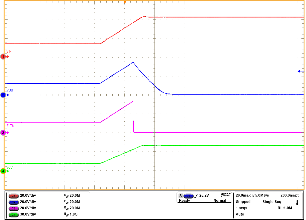
The TPS1641x implements overvoltage protection to protect the load from input overvoltage conditions. A resistor divider can be connected from the IN pin of device to configure the overvoltage protection setpoint. The device turns off the internal FET and asserts the FLT pin as the voltage at OVP pin goes above VOVPR, and as the OVP pin voltage falls below VOVPF, the internal FET is turned ON and FLT pin is de-asserted. See the Section 7.5 table for VOVPF and VOVPR and Section 7.6 for tOVP_entry_dly and tOVP_exit_dly timings for overvoltage protection input. Figure 8-3 illustrates the OVP input in TPS1641x devices. Figure 8-4 shows the overvoltage response.
 Figure 8-3 OVP Input in TPS1641x
 Figure 8-4 Overvoltage Protection
Response for IN Voltage 12 V to 40 V
Figure 8-4 Overvoltage Protection
Response for IN Voltage 12 V to 40 VVcc and FLT pins of the device are rated up to 60 V, and the FLT pin can be used to drive an external PFET transistor and provide protection from 60-V overvoltage at input as shown in Figure 8-5.
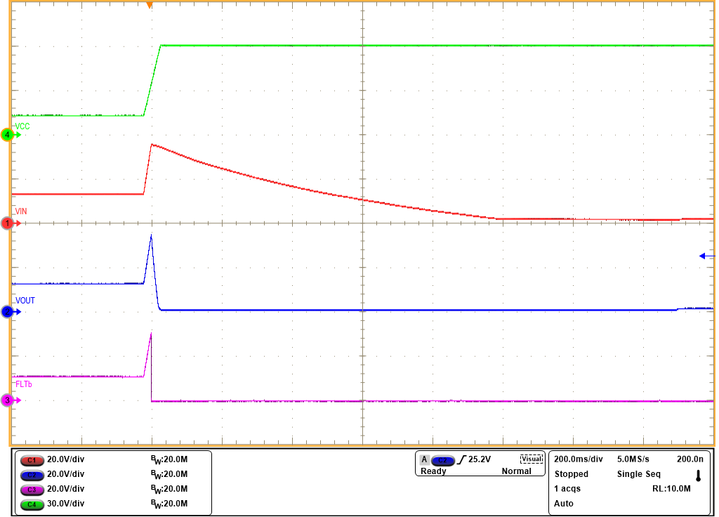
 Figure 8-5 Overvoltage (up to 60 V)
Protection with External PFET
Figure 8-5 Overvoltage (up to 60 V)
Protection with External PFETTo disable the overvoltage input, connect OVP to GND. If the OVP pin is left open, the device turns off the internal FET.
 Figure 8-6 Overvoltage Response with
External PFET for IN Voltage from 12 V to 60 V
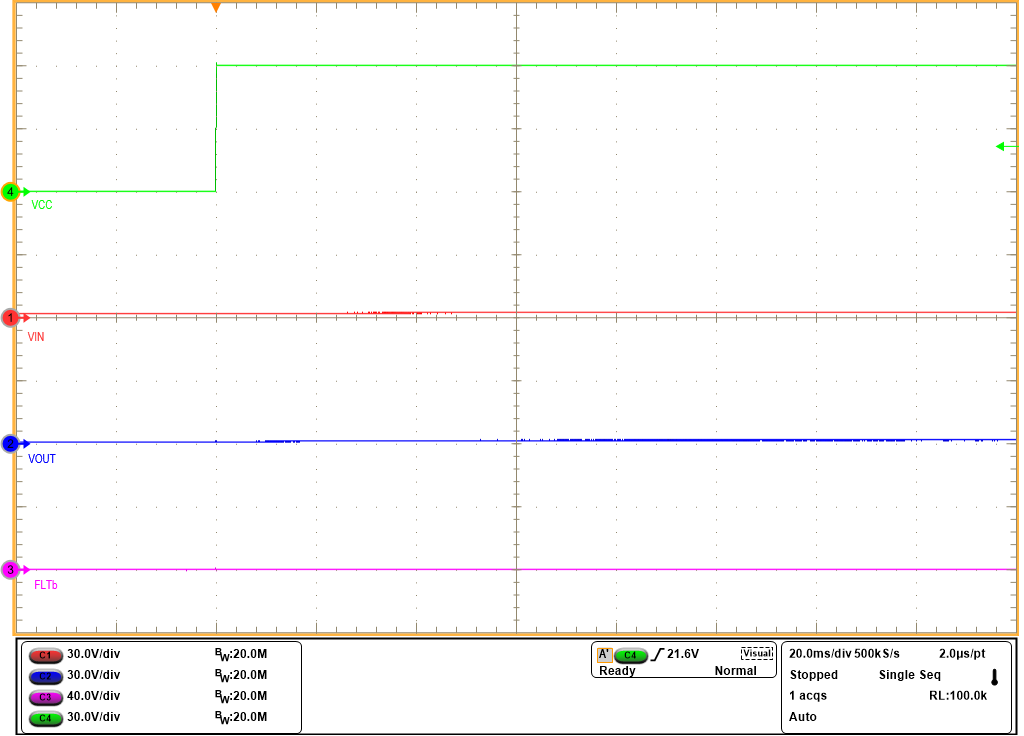
 Figure 8-7 Hot Plugin with External
PFET for 60-V Input