SLVSGF4B june 2022 – may 2023 TPS1641
PRODUCTION DATA
- 1 Features
- 2 Applications
- 3 Description
- 4 Revision History
- 5 Device Comparison Table
- 6 Pin Configuration and Functions
- 7 Specifications
-
8 Detailed Description
- 8.1 Overview
- 8.2 Functional Block Diagram
- 8.3
Feature Description
- 8.3.1 Enable and Shutdown Input (EN/SHDN)
- 8.3.2 Overvoltage Protection (OVP)
- 8.3.3 Output Slew Rate and Inrush Current Control (dVdt)
- 8.3.4 Active Current Limiting (ILIM) With the TPS16412, TPS16413, TPS16416, and TPS16417
- 8.3.5 Active Power Limiting (PLIM) With the TPS16410, TPS16411, TPS16414, and TPS16415
- 8.3.6 Overcurrent Protection (IOCP) and Blanking Time (IDLY or PDLY) for Transient Loads
- 8.3.7 Fast-Trip and Short-Circuit Protection
- 8.3.8 Analog Load Current Monitor (IMON) on the IOCP Pin
- 8.3.9 IN to OUT Short Detection (TPS16410, TPS16411, TPS16412, and TPS16413)
- 8.3.10 Thermal Shutdown and Overtemperature Protection
- 8.3.11 Fault Response and Indication (FLT)
- 8.4 Device Functional Modes
- 9 Application and Implementation
- 10Device and Documentation Support
- 11Mechanical, Packaging, and Orderable Information
Package Options
Mechanical Data (Package|Pins)
- DRC|10
Thermal pad, mechanical data (Package|Pins)
- DRC|10
Orderable Information
8.3.5 Active Power Limiting (PLIM) With the TPS16410, TPS16411, TPS16414, and TPS16415
The TPS16410, TPS16411, TPS16414, and TPS16415 devices respond to output overcurrent or overload conditions by actively limiting the output power. The devices first provide a blanking time configured by capacitance on PDLY pin. During this blanking time, the device can provide a current up to IOCP value. After the end of this blanking time, the devices limit power to PLIM value. Power limit can be set by connecting a resistor on the PLIM pin. During power limiting, if the output power goes below PLIM (POUT < PLIM), the device resets the PDLY timer and restarts the PDLY timer when POUT > PLIM. Use Equation 4 to calculate the value of resistor for power limiting. The device is rated for 1.8-A continuous current, TI recommends to set PLIM < VIN × 1.8 A and PLIM < 0.9 × VOUT × IOCP
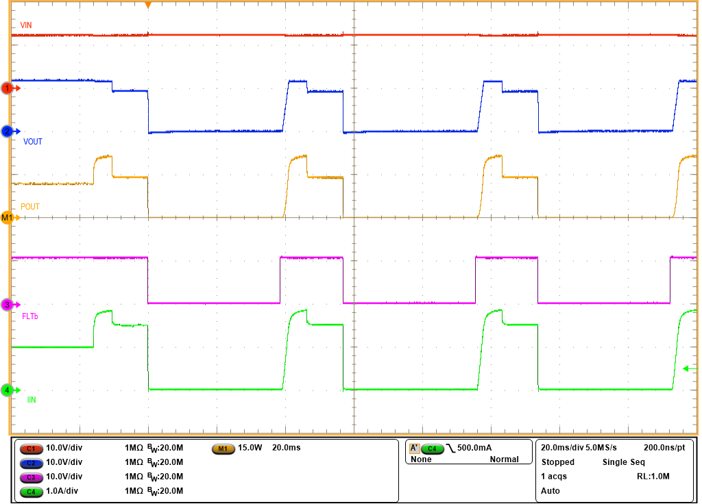
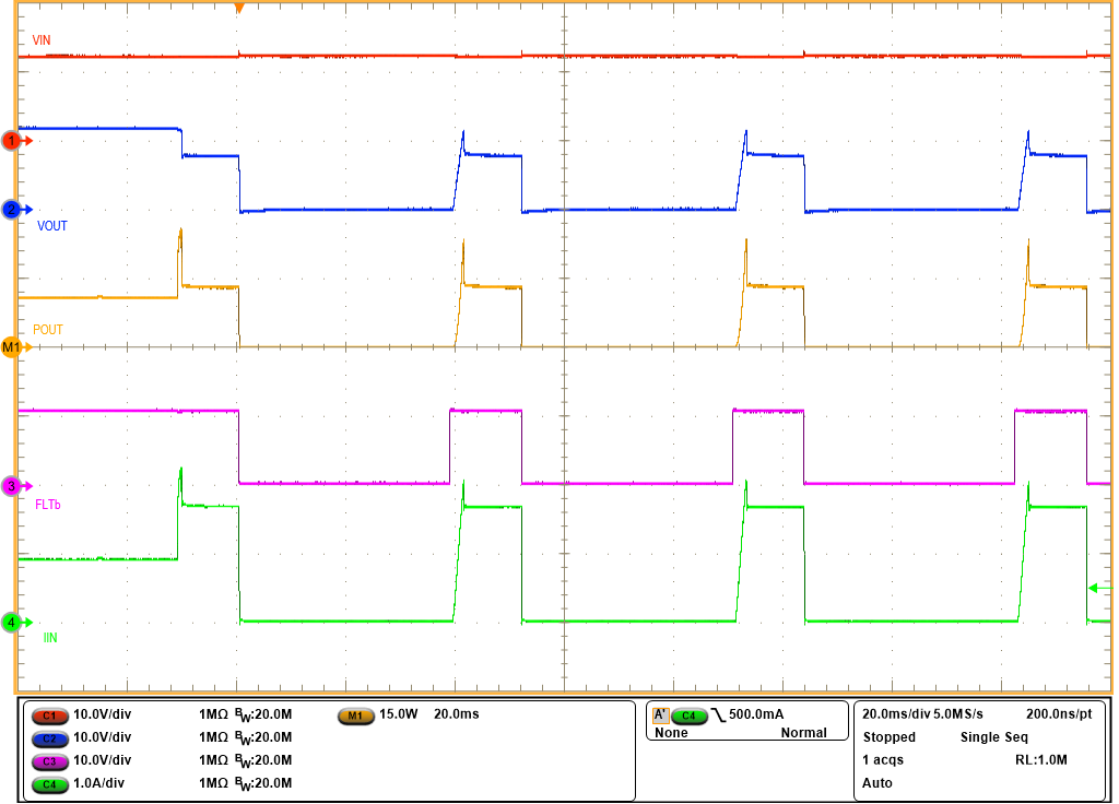
Figure 8-12 illustrates the power limiting in the TPS16410 and TPS16411 devices for IOUT < IOCP and IOCP ≤ IOUT < Ifast-trip.
 Figure 8-12 Power Limiting
(IOUT < IOCP)
 Figure 8-13 Power Limiting
(IOCP ≤ IOUT < Ifast-trip)
Figure 8-13 Power Limiting
(IOCP ≤ IOUT < Ifast-trip)During power limiting, the device dissipates a power of (VIN – VOUT) × IOUT and the device gets heated up. If the junction temperature of device reaches thermal shutdown temperature (TTSD), the device turns off the internal FET. If the device does not go into thermal shutdown, the internal FET is turned off after a duration of tPLIM-DUR. After the internal FET is turned off, the TPS16410 and TPS16414 devices auto-retry while the TPS16411 and TPS16415 device latch off. If PLIM is connected to GND or left open, the device turns-off the internal FET. If the PDLY pin is left open or connected to GND, device provides tPLIM-DUR = 155 ms unless the device enters thermal shutdown. Table 8-2 summarizes the device behavior for different output power and current.
| Output Power (POUT) or Output Current (IOUT) | Device Response |
|---|---|
| POUT < PLIM | The device provides power up to PLIM. |
PLIM ≤ POUT and IOUT < IOCP |
The device provides current up to IOCP for a duration of PDLY and then limits power to PLIM for a maximum duration of tPLIM-DUR. |
| IOCP ≤ IOUT < Ifast-trip | The device limits current to PLIM for a maximum duration of tPLIM-DUR. |
| Ifast-trip ≤ IOUT < ISCP | The device turns off the internal FET after a delay of tfast-trip. |
| ISCP ≤ IOUT | The device turns off the internal FET after a delay of tSCP_dly. |