SLVSET9F September 2018 – February 2023 TPS1663
PRODUCTION DATA
- 1 Features
- 2 Applications
- 3 Description
- 4 Revision History
- 5 Device Comparison Table
- 6 Pin Configuration and Functions
- 7 Specifications
- 8 Parameter Measurement Information
-
9 Detailed Description
- 9.1 Overview
- 9.2 Functional Block Diagram
- 9.3
Feature Description
- 9.3.1 Hot Plug-In and In-Rush Current Control
- 9.3.2 Undervoltage Lockout (UVLO)
- 9.3.3 Overvoltage Protection (OVP)
- 9.3.4 Overload and Short Circuit Protection
- 9.3.5 Output Power Limiting, PLIM (TPS16632 Only)
- 9.3.6 Current Monitoring Output (IMON)
- 9.3.7 FAULT Response (FLT)
- 9.3.8 Power Good Output (PGOOD)
- 9.3.9 IN, P_IN, OUT and GND Pins
- 9.3.10 Thermal Shutdown
- 9.3.11 Low Current Shutdown Control (SHDN)
- 9.4 Device Functional Modes
- 10Application and Implementation
- 11Device and Documentation Support
- 12Mechanical, Packaging, and Orderable Information
Package Options
Refer to the PDF data sheet for device specific package drawings
Mechanical Data (Package|Pins)
- RGE|24
- PWP|20
Thermal pad, mechanical data (Package|Pins)
Orderable Information
9.3.3 Overvoltage Protection (OVP)
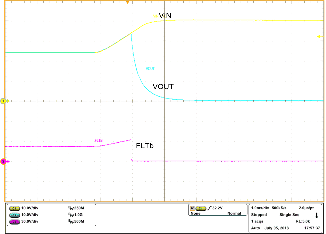
The TPS1663x incorporate circuitry to protect the system during overvoltage conditions. The TPS16630 features an accurate ± 2% adjustable overvoltage cut off functionality. A voltage more than V(OVPR) on OVP pin turns off the internal FET and protects the downstream load. To program the OVP threshold externally, connect a resistor divider from IN supply to OVP terminal to GND as shown in GUID-EFA225D6-4B07-4237-99E9-57A72AEBFA09.html#T5464742-7. The TPS16632 features an internally fixed 39-V maximum overvoltage clamp V(OVC) functionality. The TPS16632 clamps the output voltage to V(OVC), when the input voltage exceeds 40 V. During the output voltage clamp operation, the power dissipation in the internal MOSFET is PD = (V(IN) – V(OVC)) × I(OUT). Excess power dissipation for a prolonged period can increase the device temperature. To avoid this, the internal FET is operated in overvoltage clamp for a maximum duration of tOVC(dly), 162 msec (typical). After this duration, the internal FET is turned OFF and the subsequent operation of the device depends on the MODE configuration (auto-retry or latch off) setting as per the Table 9-1.
#TESTD illustrates the overvoltage cut-off functionality and #TESTZ illustrates the overvoltage clamp functionality. FLT is asserted after a delay of 617 µs (typical) after entering in overvoltage clamp mode and remains asserted until the overvoltage fault is removed.

| TPS16630 | OVP Setting at 33 V | |

| TPS16632 | COUT = 10 µF, FLT connected to VOUT | RLOAD = 30 Ω |