SLVSDO6C
August 2017 – June 2019
TPS1H000-Q1
PRODUCTION DATA.
1
Features
2
Applications
3
Description
Device Images
Typical Block Diagram
Current-Limit Protection in Auto-Retry Mode
4
Revision History
5
Pin Configuration and Functions
Pin Functions
6
Specifications
6.1
Absolute Maximum Ratings
6.2
ESD Ratings
6.3
Recommended Operating Conditions
6.4
Thermal Information
6.5
Electrical Characteristics
6.6
Switching Characteristics
6.7
Typical Characteristics
7
Detailed Description
7.1
Overview
7.2
Functional Block Diagram
7.3
Feature Description
7.3.1
Current Limit
7.3.2
DELAY Pin Configuration
7.3.2.1
Holding Mode
7.3.2.2
Latch-Off Mode
7.3.2.3
Auto-Retry Mode
7.3.3
Standalone Operation
7.3.4
Fault Truth Table
7.3.5
Full Diagnostics
7.3.5.1
Short-to-GND and Overload Detection
7.3.5.2
Open-Load Detection
7.3.5.2.1
Output On
7.3.5.2.2
Output Off
7.3.5.3
Short-to-Battery Detection
7.3.5.4
Thermal Fault Detection
7.3.5.4.1
Thermal Shutdown
7.3.5.4.2
Thermal Swing
7.3.5.4.3
Fault Report Holding
7.3.6
Full Protections
7.3.6.1
UVLO Protection
7.3.6.2
Inductive Load Switching Off Clamp
7.3.6.3
Loss-of-GND Protection
7.3.6.4
Loss-of-Power-Supply Protection
7.3.6.5
Reverse-Current Protection
7.3.6.6
MCU I/O Protection
7.4
Device Functional Modes
7.4.1
Working Modes
7.4.1.1
Normal Mode
7.4.1.2
Standby Mode
7.4.1.3
Standby Mode With Diagnostics
8
Application and Implementation
8.1
Application Information
8.2
Typical Application
8.2.1
Design Requirements
8.2.2
Detailed Design Procedure
8.2.3
Application Curves
9
Power Supply Recommendations
10
Layout
10.1
Layout Guidelines
10.2
Layout Example
11
Device and Documentation Support
11.1
Receiving Notification of Documentation Updates
11.2
Community Resources
11.3
Trademarks
11.4
Electrostatic Discharge Caution
11.5
Glossary
12
Mechanical, Packaging, and Orderable Information
Package Options
Mechanical Data (Package|Pins)
DGN|8
MPDS046G
Thermal pad, mechanical data (Package|Pins)
DGN|8
PPTD362A
Orderable Information
slvsdo6c_oa
slvsdo6c_pm
6.7
Typical Characteristics
Figure 3.
UVLO Voltage Threshold
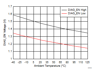
Figure 5.
DIAG_EN Voltage Threshold
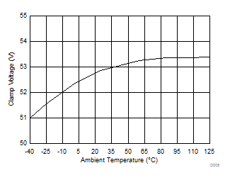
Figure 7.
Drain-to-Source Clamp Voltage
I
OUT
= 50 mA
Figure 9.
Current-Limit Accuracy at 50 mA
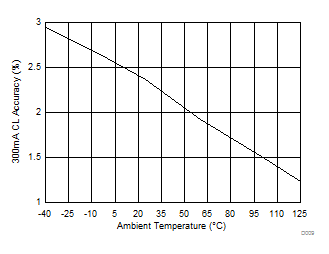
I
OUT
= 300 mA
Figure 11.
Current-Limit Accuracy at 300 mA
Figure 4.
IN Voltage Threshold
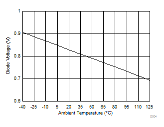
Figure 6.
Body-Diode Forward Voltage
Figure 8.
FET On-Resistance
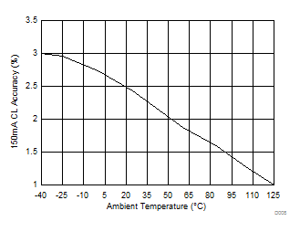
I
OUT
= 150 mA
Figure 10.
Current-Limit Accuracy at 150 mA
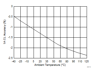
I
OUT
= 1 A
Figure 12.
Current-Limit Accuracy at 1 A