SLVSEE0D February   2018  – September 2021 TPS1H200A-Q1

PRODUCTION DATA  

  1. Features
  2. Applications
  3. Description
  4. Revision History
  5. Pin Configuration and Functions
  6. Specifications
    1. 6.1 Absolute Maximum Ratings
    2. 6.2 ESD Ratings
    3. 6.3 Recommended Operating Conditions
    4. 6.4 Thermal Information
    5. 6.5 Electrical Characteristics
    6. 6.6 Switching Characteristics
    7. 6.7 Typical Characteristics
  7. Detailed Description
    1. 7.1 Overview
    2. 7.2 Functional Block Diagram
    3. 7.3 Feature Description
      1. 7.3.1 Current limit
      2. 7.3.2 DELAY Pin Configuration
        1. 7.3.2.1 Holding Mode
        2. 7.3.2.2 Latch-Off Mode
        3. 7.3.2.3 Auto-Retry Mode
      3. 7.3.3 Stand-alone Operation
      4. 7.3.4 Fault Truth Table
      5. 7.3.5 Full Diagnostics
        1. 7.3.5.1 Short-to-GND and Overload Detection
        2. 7.3.5.2 Open-Load Detection
          1. 7.3.5.2.1 Output On
          2. 7.3.5.2.2 Output Off
        3. 7.3.5.3 Short-to-Battery Detection
        4. 7.3.5.4 Thermal Fault Detection
          1. 7.3.5.4.1 Thermal Shutdown
          2. 7.3.5.4.2 Thermal Swing
          3. 7.3.5.4.3 Fault Report Holding
      6. 7.3.6 Full Protections
        1. 7.3.6.1 UVLO Protection
        2. 7.3.6.2 Inductive Load Switching Off Clamp
        3. 7.3.6.3 Loss-of-GND Protection
        4. 7.3.6.4 Loss-of-Power-Supply Protection
        5. 7.3.6.5 Reverse-Current Protection
        6. 7.3.6.6 MCU I/O Protection
    4. 7.4 Device Functional Modes
      1. 7.4.1 Working Modes
        1. 7.4.1.1 Normal Mode
        2. 7.4.1.2 Standby Mode
        3. 7.4.1.3 Standby Mode With Diagnostics
  8. Application and Implementation
    1. 8.1 Application Information
    2. 8.2 Typical Application
      1. 8.2.1 Design Requirements
      2. 8.2.2 Detailed Design Procedure
      3. 8.2.3 Application Curves
  9. Power Supply Recommendations
  10. 10Layout
    1. 10.1 Layout Guidelines
    2. 10.2 Layout Example
  11. 11Device and Documentation Support
    1. 11.1 Documentation Support
      1. 11.1.1 Related Documentation
    2. 11.2 Receiving Notification of Documentation Updates
    3. 11.3 Support Resources
    4. 11.4 Trademarks
    5. 11.5 Electrostatic Discharge Caution
    6. 11.6 Glossary
  12. 12Mechanical, Packaging, and Orderable Information

Package Options

Mechanical Data (Package|Pins)
Thermal pad, mechanical data (Package|Pins)
Orderable Information

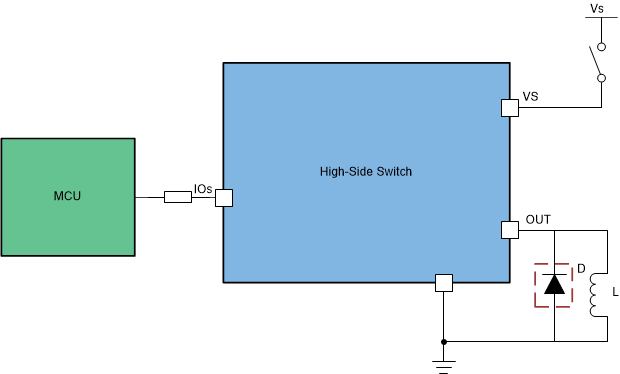
Loss-of-Power-Supply Protection

When a loss-of-power-supply occurs, the output shuts down, regardless of whether the IN pin is high or low. For a resistive or a capacitive load, the loss-of-power-supply has no risk. But for a charged inductive load, the current is driven from all the logic control pins to maintain the inductance current. To protect the system in this condition, TI recommends protection with an external free-wheeling diode.
GUID-76D3800B-F903-40AA-9B67-6FECEEA0E905-low.gifFigure 7-16 Protection for Loss of Power Supply