SLVSE18B June   2019  – February 2023 TPS1HB35-Q1

PRODUCTION DATA  

  1. Features
  2. Applications
  3. Description
  4. Revision History
  5. Device Comparison Table
  6. Pin Configuration and Functions
    1. 6.1 Recommended Connections for Unused Pins
  7. Specifications
    1. 7.1 Recommended Operating Conditions
    2. 7.2 Electrical Characteristics
    3. 7.3 Absolute Maximum Ratings
    4. 7.4 ESD Ratings
    5. 7.5 Thermal Information
    6. 7.6 SNS Timing Characteristics
    7. 7.7 Switching Characteristics
    8. 7.8 Typical Characteristics
  8. Parameter Measurement Information
  9. Detailed Description
    1. 9.1 Overview
    2. 9.2 Functional Block Diagram
    3. 9.3 Feature Description
      1. 9.3.1 Protection Mechanisms
        1. 9.3.1.1 Thermal Shutdown
        2. 9.3.1.2 Current Limit
          1. 9.3.1.2.1 Current Limit Foldback
          2. 9.3.1.2.2 Programmable Current Limit
          3. 9.3.1.2.3 Undervoltage Lockout (UVLO)
          4. 9.3.1.2.4 VBB During Short-to-Ground
        3. 9.3.1.3 Voltage Transients
          1. 9.3.1.3.1 Load Dump
          2. 9.3.1.3.2 Driving Inductive Loads
        4. 9.3.1.4 Reverse Battery
        5. 9.3.1.5 Current Limit Behavior
        6. 9.3.1.6 Fault Event – Timing Diagrams
      2. 9.3.2 Diagnostic Mechanisms
        1. 9.3.2.1 VOUT Short-to-Battery and Open-Load
          1. 9.3.2.1.1 Detection With Switch Enabled
          2. 9.3.2.1.2 Detection With Switch Disabled
        2. 9.3.2.2 SNS Output
          1. 9.3.2.2.1 RSNS Value
            1. 9.3.2.2.1.1 High Accuracy Load Current Sense
            2. 9.3.2.2.1.2 SNS Output Filter
        3. 9.3.2.3 Fault Indication and SNS Mux
        4. 9.3.2.4 Resistor Sharing
        5. 9.3.2.5 High-Frequency, Low Duty-Cycle Current Sensing
    4. 9.4 Device Functional Modes
      1. 9.4.1 Off
      2. 9.4.2 Standby
      3. 9.4.3 Diagnostic
      4. 9.4.4 Standby Delay
      5. 9.4.5 Active
      6. 9.4.6 Fault
  10. 10Application and Implementation
    1. 10.1 Application Information
      1. 10.1.1 Ground Protection Network
      2. 10.1.2 Interface With Microcontroller
      3. 10.1.3 I/O Protection
      4. 10.1.4 Inverse Current
      5. 10.1.5 Loss of GND
      6. 10.1.6 Automotive Standards
        1. 10.1.6.1 ISO7637-2
        2. 10.1.6.2 AEC-Q100-012 Short Circuit Reliability
      7. 10.1.7 Thermal Information
    2. 10.2 Typical Application
      1. 10.2.1 Design Requirements
      2. 10.2.2 Detailed Design Procedure
        1. 10.2.2.1 Thermal Considerations
        2. 10.2.2.2 RILIM Calculation
        3. 10.2.2.3 Diagnostics
          1. 10.2.2.3.1 Selecting the RISNS Value
    3. 10.3 Typical Application
      1. 10.3.1 Design Requirements
      2. 10.3.2 Detailed Design Procedure
      3. 10.3.3 Application Curves
    4. 10.4 Power Supply Recommendations
    5. 10.5 Layout
      1. 10.5.1 Layout Guidelines
      2. 10.5.2 Layout Example
  11. 11Device and Documentation Support
    1. 11.1 Documentation Support
      1. 11.1.1 Related Documentation
    2. 11.2 Receiving Notification of Documentation Updates
    3. 11.3 Support Resources
    4. 11.4 Trademarks
    5. 11.5 Electrostatic Discharge Caution
    6. 11.6 Glossary
  12. 12Mechanical, Packaging, and Orderable Information

Package Options

Mechanical Data (Package|Pins)
Thermal pad, mechanical data (Package|Pins)
Orderable Information

Fault Event – Timing Diagrams

Note:

All timing diagrams assume that the SEL1 pin is low.

The LATCH, DIA_EN, and EN pins are controlled by the user. The timing diagrams represent a possible use-case.

#SLVSE157371 shows the immediate current limit switch off behavior. The diagram also illustrates the retry behavior. As shown, the switch will remain latched off until the LATCH pin is low.
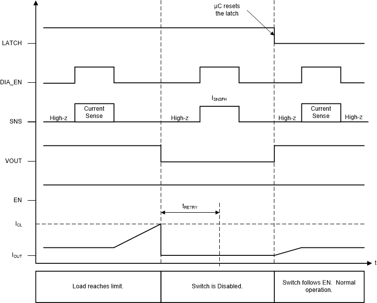
GUID-9AD29FF8-D3CC-47CD-A8A3-A880A9B2B84E-low.gifFigure 9-6 Current Limit – Version A and B - Latched Behavior

#SLVSE156584 shows the immediate current limit switch off behavior. In this example, LATCH is tied to GND; hence, the switch will retry after the fault is cleared and tRETRY has expired.
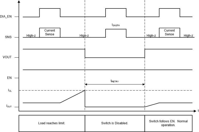
GUID-0788BB4A-26C0-4B67-B407-2CADBABC76F5-low.gifFigure 9-7 Current Limit - Version A and B - LATCH = 0

#SLVSDZ36421 shows the active current behavior of version C. In version C, the switch will not shutdown until thermal shutdown is reached.
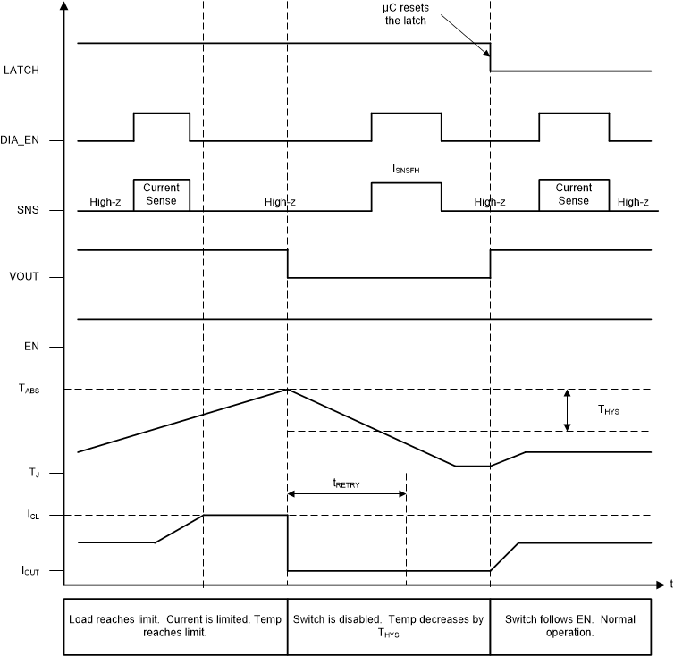
GUID-20200908-CA0I-089G-DFVV-HV87CGZKXZHF-low.gif Figure 9-8 Current Limit – Version C - Latched Behavior

#SLVSDZ33291 shows the active current behavior of version C. The switch will not shutdown until thermal shutdown is tripped. In this example, LATCH is tied to GND.
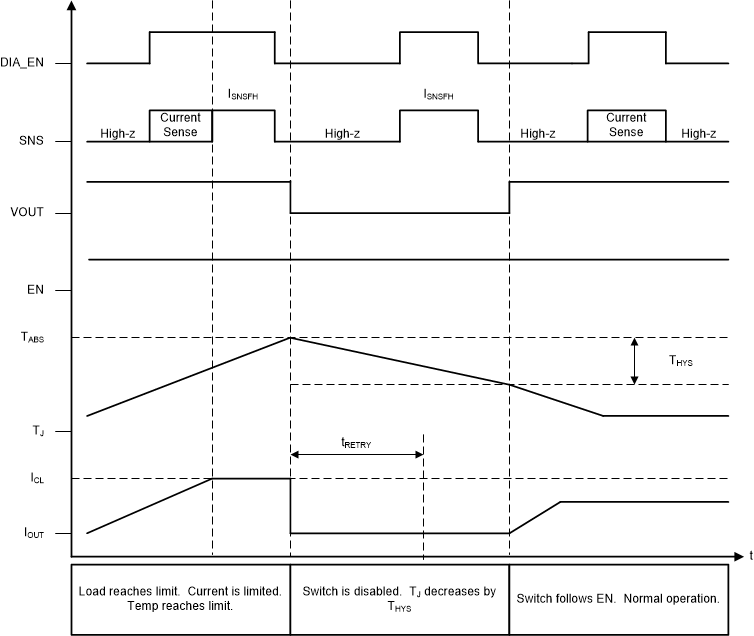
GUID-20200908-CA0I-ZTQC-SPBX-HQ0VHKLJ60J4-low.gif Figure 9-9 Current Limit – Version C - LATCH = 0

When the switch retries after a shutdown event, the SNS fault indication will remain until VOUT has risen to VBB – 1.8 V. After VOUT has risen, the SNS fault indication is reset and current sensing is available. If there is a short-to-ground and VOUT is not able to rise, the SNS fault indication will remain indefinitely. #SLVSE158822 illustrates auto-retry behavior and provides a zoomed-in view of the fault indication during retry.

Note:

#SLVSE158822 assumes that tRETRY has expired by the time that TJ reaches the hysteresis threshold.

LATCH = 0 V and DIA_EN = 5 V
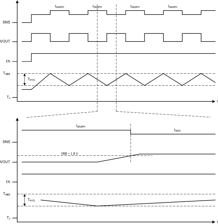
GUID-FA5799DC-6488-44A4-8D74-9A7E40BBB8C4-low.gifFigure 9-10 Fault Indication During Retry