SLVSGZ7B May   2023  – October 2023 TPS2000E , TPS2001E , TPS2068E , TPS2069E

PRODUCTION DATA  

  1.   1
  2. Features
  3. Applications
  4. Description
  5. Device Comparison Table
  6. Pin Configuration and Functions
  7. Specifications
    1. 6.1 Absolute Maximum Ratings
    2. 6.2 ESD Ratings
    3. 6.3 Recommended Operating Conditions
    4. 6.4 Thermal Information
    5. 6.5 Electrical Characteristics
    6.     13
    7. 6.6 Typical Characteristics
  8. Detailed Description
    1. 7.1 Overview
    2. 7.2 Functional Block Diagram
    3. 7.3 Feature Description
      1. 7.3.1 Undervoltage Lockout
      2. 7.3.2 Enable
      3. 7.3.3 Internal Charge Pump
      4. 7.3.4 Current Limit
      5. 7.3.5 FLT
      6. 7.3.6 Output Discharge
    4. 7.4 Device Functional Modes
      1. 7.4.1 Shutdown Mode
      2. 7.4.2 Active Mode
  9. Application and Implementation
    1. 8.1 Application Information
    2. 8.2 Typical Application
      1. 8.2.1 Design Requirements
      2. 8.2.2 Detailed Design Procedure
        1. 8.2.2.1 Input and Output Capacitance
      3. 8.2.3 Application Curves
    3. 8.3 Power Supply Recommendations
    4. 8.4 Layout
      1. 8.4.1 Layout Guidelines
      2. 8.4.2 Layout Example
  10. Device and Documentation Support
    1. 9.1 Documentation Support
    2. 9.2 Receiving Notification of Documentation Updates
    3. 9.3 Support Resources
    4. 9.4 Trademarks
    5. 9.5 Electrostatic Discharge Caution
    6. 9.6 Glossary
  11. 10Revision History
  12. 11Mechanical, Packaging, and Orderable Information

Package Options

Mechanical Data (Package|Pins)
Thermal pad, mechanical data (Package|Pins)
Orderable Information

Application Curves

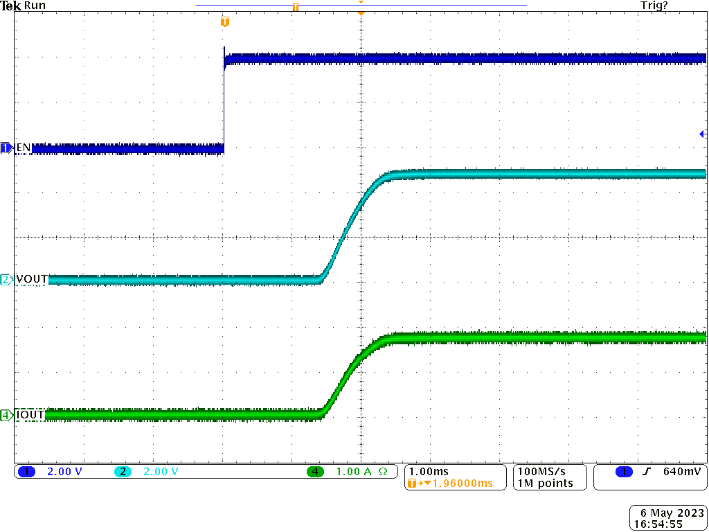
GUID-20230508-SS0I-B76K-J8W3-VFSQTNN2RNG6-low.png
VIN = 5 V VEN = 4 V RLoad = 2.5 Ω
Figure 8-2 Turnon Delay and Rise Time
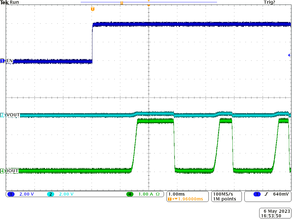
GUID-20230508-SS0I-QG8Q-8RCQ-FMCT33MNPN6Z-low.png
VIN = 5 V VEN = 4 V OUT short to GND
Figure 8-4 TPS2001E Enable into Output Short
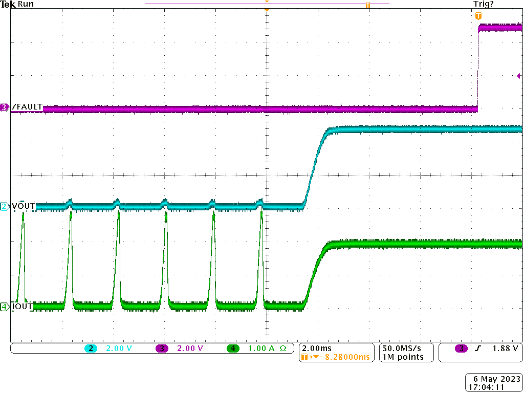
GUID-20230508-SS0I-812B-Q4Z1-43GVV5RMFHCH-low.png
VIN = 5 V
Figure 8-6 TPS2001E Output Short to Full Load
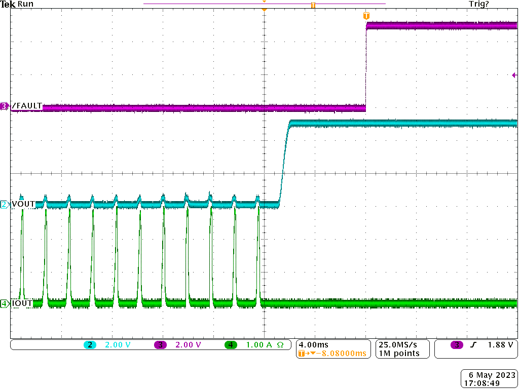
GUID-20230508-SS0I-ZR0P-PQR7-DX9MVWS5QFPC-low.png
VIN = 5 V
Figure 8-8 TPS2001E Output Short to No Load
GUID-20230508-SS0I-V8KQ-G4TC-WPNWSPFCVP5Q-low.png
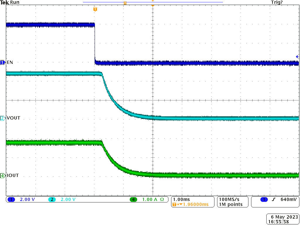
VIN = 5 V VEN = 4 V RLoad = 2.5 Ω
Figure 8-3 Turnoff Delay and Fall Time
GUID-20230508-SS0I-RTZP-NN20-DCFPPTWPSQM4-low.png
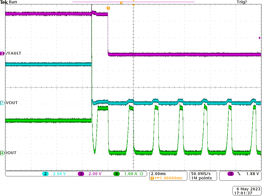
VIN = 5 V
Figure 8-5 TPS2001E Full Load to Output Short
GUID-20230508-SS0I-CMB7-DNV5-FX3PWVPNKQX5-low.png
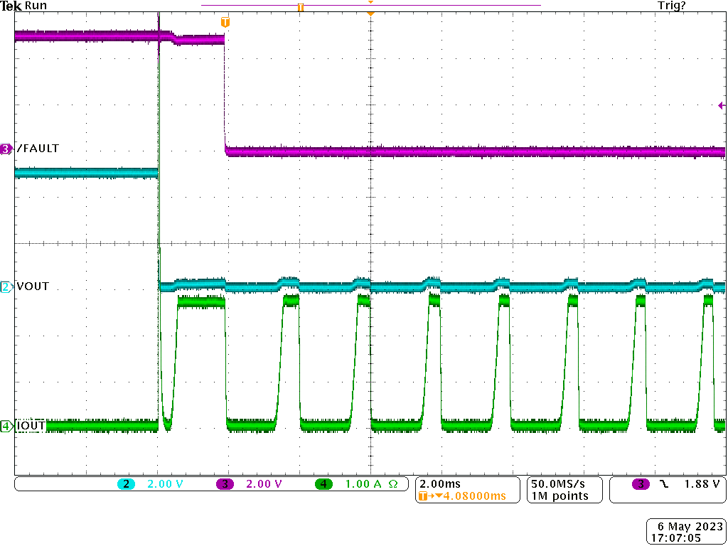
VIN = 5 V
Figure 8-7 TPS2001E No Load to Output Short