SLVSAX6H October 2011 – December 2015 TPS2002C , TPS2003C , TPS2052C , TPS2060C , TPS2062C , TPS2062C-2 , TPS2064C , TPS2064C-2 , TPS2066C , TPS2066C-2
PRODUCTION DATA.
- 1 Features
- 2 Applications
- 3 Description
- 4 Revision History
- 5 Device Comparison Table
- 6 Pin Configuration and Functions
- 7 Specifications
- 8 Parameter Measurement Information
- 9 Detailed Description
- 10Application and Implementation
- 11Power Supply Recommendations
- 12Layout
- 13Device and Documentation Support
- 14Mechanical, Packaging, and Orderable Information
Package Options
Mechanical Data (Package|Pins)
- DRC|10
Thermal pad, mechanical data (Package|Pins)
Orderable Information
10 Application and Implementation
NOTE
Information in the following applications sections is not part of the TI component specification, and TI does not warrant its accuracy or completeness. TI’s customers are responsible for determining suitability of components for their purposes. Customers should validate and test their design implementation to confirm system functionality.
10.1 Application Information
The universal serial bus (USB) interface is a 12-Mb/s, or 1.5-Mb/s, multiplexed serial bus designed for low-to-medium bandwidth PC peripherals (for example, keyboards, printers, scanners, and mice). The four-wire USB interface is conceived for dynamic attach-detach (hot plug-unplug) of peripherals. Two lines are provided for differential data, and two lines are provided for 5-V power distribution.
USB data is a 3.3-V level signal, but power is distributed at 5 V to allow for voltage drops in cases where power is distributed through more than one hub across long cables. Each function must provide its own regulated 3.3 V from the 5-V input or its own internal power supply.
The USB specification defines the following five classes of devices, each differentiated by power-consumption requirements:
- Hosts or self-powered hubs (SPH)
- Bus-powered hubs (BPH)
- Low-power, bus-powered functions
- High-power, bus-powered functions
- Self-powered functions
Self-powered and bus-powered hubs distribute data and power to downstream functions. The TPS20xxC and TPS20xxC-2 can provide power distribution solutions to many of these device classes.
10.2 Typical Application
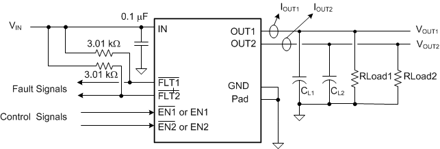
 Figure 31. Typical Application Circuit
10.2.1 Design Requirements
Table 3 shows the design requirements for the typical application.
Table 3. Design Parameters
| PARAMETER | VALUE |
|---|---|
| Input voltage | 5 V |
| Output voltage 1 | 5 V |
| Output voltage 2 | 5 V |
| Current limit | 1 A |
10.2.2 Detailed Design Procedure
10.2.2.1 Input and Output Capacitance
Input and output capacitance improves the performance of the device. For all applications, TI recommends placing a 0.1-µF or greater ceramic bypass capacitor between IN and GND as close as possible to the device for local noise de-coupling. The actual capacitance should be optimized for the particular application. This precaution reduces ringing on the input due to power-supply transients. Additional input capacitance may be needed on the input to reduce the overshoot voltage from exceeding the absolute maximum voltage of the device during heavy transients.
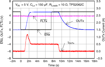
A 120-µF minimum output capacitance is required when implementing USB standard applications. Typically this uses a 150-µF electrolytic capacitor. If the application does not require 120 µF of output capacitance, a minimum of 10-µF ceramic capacitor on the output is recommended to reduce the transient negative voltage on OUTx pin caused by load inductance during a short circuit. The transient negative voltage should be less than 1.5 V for
10 µs.
10.2.3 Application Curves

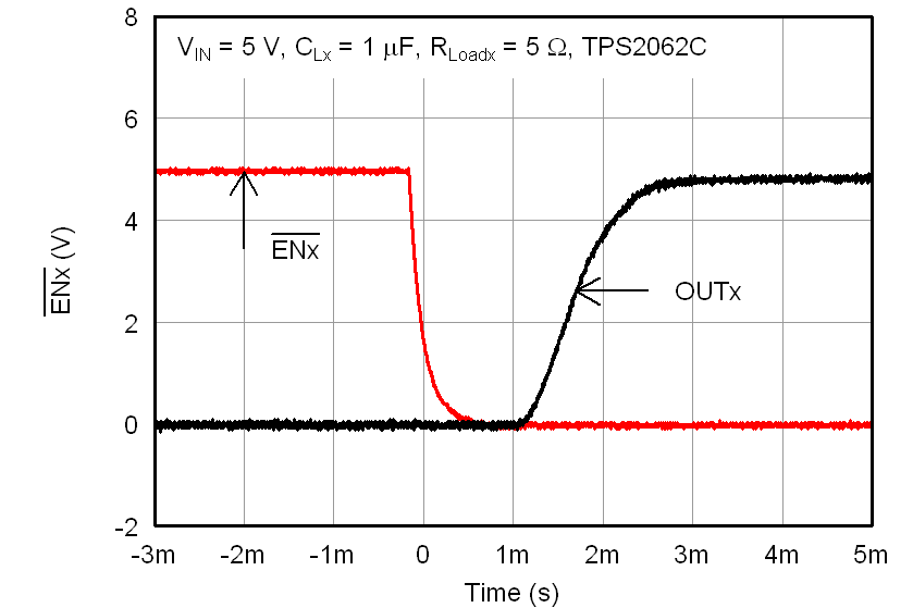
Rise Time With 1-μF Load
