SLVS782D November   2007  – October 2020 TPS2041B-Q1 , TPS2042B-Q1 , TPS2051B-Q1

PRODUCTION DATA  

  1. Features
  2. Applications
  3. Description
  4. Revision History
  5. Pin Configuration and Functions
  6. Specifications
    1. 6.1 Absolute Maximum Ratings
    2. 6.2 ESD Ratings
    3. 6.3 Recommended Operating Conditions
    4. 6.4 Thermal Information
    5. 6.5 Electrical Characteristics
    6. 6.6 Typical Characteristics
  7. Parameter Measurement Information
  8. Detailed Description
    1. 8.1 Overview
    2. 8.2 Functional Block Diagrams
    3. 8.3 Feature Description
      1. 8.3.1 Power Switch
      2. 8.3.2 Charge Pump
      3. 8.3.3 Driver
      4. 8.3.4 Enable ( ENx)
      5. 8.3.5 Enable (EN)
      6. 8.3.6 Overcurrent ( OCx)
      7. 8.3.7 Current Sense
      8. 8.3.8 Thermal Sense
      9. 8.3.9 Undervoltage Lockout (UVLO)
    4. 8.4 Device Functional Modes
  9. Application and Implementation
    1. 9.1 Application Information
      1. 9.1.1 Universal Serial Bus (USB) Applications
    2. 9.2 Typical Applications
      1. 9.2.1 TPS2042B-Q1 Typical Application
        1. 9.2.1.1 Design Requirements
        2. 9.2.1.2 Detailed Design Procedure
          1. 9.2.1.2.1 Overcurrent
          2. 9.2.1.2.2 OC Response
        3. 9.2.1.3 Application Curves
      2. 9.2.2 Hosts and Self-Powered Hubs and Bus-Powered Hubs
        1. 9.2.2.1 Design Requirements
          1. 9.2.2.1.1 USB Power-Distribution Requirements
        2. 9.2.2.2 Detailed Design Procedure
          1. 9.2.2.2.1 Low-Power Bus-Powered and High-Power Bus-Powered Functions
      3. 9.2.3 Generic Hot-Plug Applications
        1. 9.2.3.1 Design Requirements
        2. 9.2.3.2 Detailed Design Procedure
  10. 10Power Supply Recommendations
  11. 11Layout
    1. 11.1 Layout Guidelines
    2. 11.2 Layout Example
    3. 11.3 Thermal Considerations
  12. 12Device and Documentation Support
    1. 12.1 Related Links
    2. 12.2 Receiving Notification of Documentation Updates
    3. 12.3 Support Resources
    4. 12.4 Trademarks
    5. 12.5 Electrostatic Discharge Caution
    6. 12.6 Glossary
  13. 13Mechanical, Packaging, and Orderable Information

Package Options

Mechanical Data (Package|Pins)
Thermal pad, mechanical data (Package|Pins)
Orderable Information

Application Curves

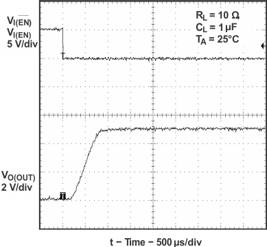
GUID-F229803D-9433-4876-AB9B-0A18A802F0C7-low.gifFigure 9-3 Turnon Delay and Rise Time With 1-µF Load
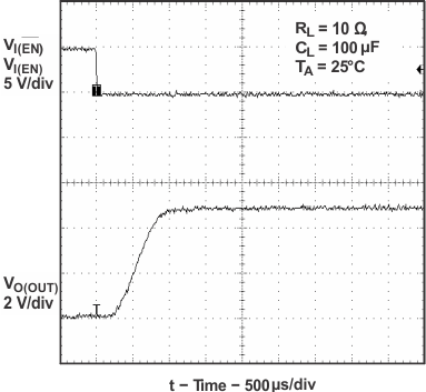
GUID-C504FC18-2C0D-4346-9BDF-788EC0DD43EF-low.gifFigure 9-5 Turnon Delay and Rise Time With 100-µF Load
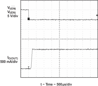
GUID-367C38BA-0779-4CB1-95D2-489A3EF42679-low.gifFigure 9-7 Short-Circuit Current, Device Enabled Into Short
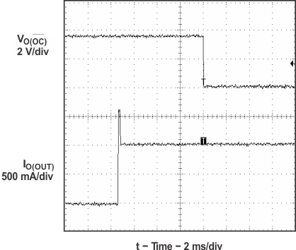
GUID-FA0C1425-8058-41AE-9B46-450B158B0688-low.gifFigure 9-9 3-Ω Load Connected to Enabled Device
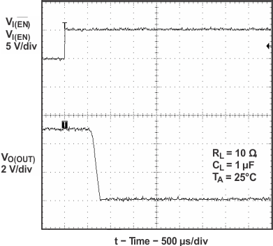
GUID-4BF7397F-62D3-4E51-8C9A-97487C9BCFF8-low.gifFigure 9-4 Turnoff Delay and Fall Time With 1-µF Load
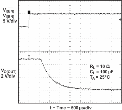
GUID-00564E8A-57AD-4081-B1B1-3BB52FD99489-low.gifFigure 9-6 Turnoff Delay and Fall Time With 100-µF Load
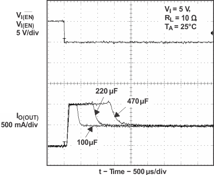
GUID-294A51B0-AE0B-4893-96D0-D0431A9382AA-low.gifFigure 9-8 Inrush Current With Different Load Capacitance
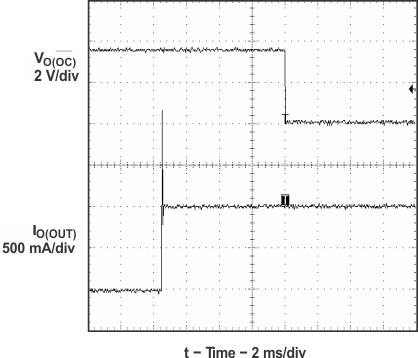
GUID-492A652E-F143-4BA9-99F9-E456AED90109-low.gifFigure 9-10 2-Ω Load Connected to Enabled Device