SLVS714B February 2007 – June 2024 TPS2062-1 , TPS2065-1 , TPS2066-1
PRODUCTION DATA
- 1
- 1 Features
- 2 Applications
- 3 Description
- 4 Pin Configuration and Functions
- 5 Specifications
- 6 Parameter Measurement Information
- 7 Detailed Description
-
8 Application and Implementation
- 8.1
Application Information
- 8.1.1 Power-Supply Considerations
- 8.1.2 OC Response
- 8.1.3 Power Dissipation and Junction Temperature
- 8.1.4 Thermal Protection
- 8.1.5 Undervoltage Lockout (UVLO)
- 8.1.6 Universal Serial Bus (USB) Applications
- 8.1.7 Host/Self-Powered and Bus-Powered Hubs
- 8.1.8 Low-Power Bus-Powered and High-Power Bus-Powered Functions
- 8.1.9 USB Power-Distribution Requirements
- 8.1.10 Generic Hot-Plug Applications
- 8.1
Application Information
- 9 Device and Documentation Support
- 10Revision History
- 11Mechanical, Packaging, and Orderable Information
Package Options
Refer to the PDF data sheet for device specific package drawings
Mechanical Data (Package|Pins)
- D|8
Thermal pad, mechanical data (Package|Pins)
Orderable Information
8.1.2 OC Response
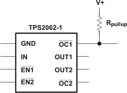
The OCx open-drain output is asserted (active low) when an overcurrent or overtemperature shutdown condition is encountered after a 10-ms deglitch timeout. The output remains asserted until the overcurrent or overtemperature condition is removed. Connecting a heavy capacitive load to an enabled device can cause a momentary overcurrent condition; however, no false reporting on OCx occurs due to the 10-ms deglitch circuit. The TPS206x-1 is designed to eliminate false overcurrent reporting. The internal overcurrent deglitch eliminates the need for external components to remove unwanted pulses. OCx is not deglitched when the switch is turned off due to an overtemperature shutdown.
 Figure 8-2 Typical Circuit for the
OC Pin