SLVS714B February 2007 – June 2024 TPS2062-1 , TPS2065-1 , TPS2066-1
PRODUCTION DATA
- 1
- 1 Features
- 2 Applications
- 3 Description
- 4 Pin Configuration and Functions
- 5 Specifications
- 6 Parameter Measurement Information
- 7 Detailed Description
-
8 Application and Implementation
- 8.1
Application Information
- 8.1.1 Power-Supply Considerations
- 8.1.2 OC Response
- 8.1.3 Power Dissipation and Junction Temperature
- 8.1.4 Thermal Protection
- 8.1.5 Undervoltage Lockout (UVLO)
- 8.1.6 Universal Serial Bus (USB) Applications
- 8.1.7 Host/Self-Powered and Bus-Powered Hubs
- 8.1.8 Low-Power Bus-Powered and High-Power Bus-Powered Functions
- 8.1.9 USB Power-Distribution Requirements
- 8.1.10 Generic Hot-Plug Applications
- 8.1
Application Information
- 9 Device and Documentation Support
- 10Revision History
- 11Mechanical, Packaging, and Orderable Information
Package Options
Refer to the PDF data sheet for device specific package drawings
Mechanical Data (Package|Pins)
- DGN|8
Thermal pad, mechanical data (Package|Pins)
- DGN|8
Orderable Information
4 Pin Configuration and Functions
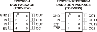
| PIN | I/O | DESCRIPTION | |||
|---|---|---|---|---|---|
| NAME | TPS2065-1 | TPS2062-1 | TPS2066-1 | ||
| EN | 4 | – | – | I | Enable input, logic high turns on power switch |
| EN1 | – | 3 | – | I | Enable input, logic low turns on channel 1 |
| EN2 | – | 4 | – | I | Enable input, logic high turns on channel 2 |
| EN1 | – | – | 3 | I | Enable input, logic high turns on channel 1 |
| EN2 | – | – | 4 | I | Enable input, logic high turns on channel 2 |
| GND | 1 | 1 | 1 | Ground connection | |
| IN | 2, 3 | 2 | 2 | I | Input voltage; connect a 0.1 μF or greater ceramic capacitor from IN to GND as close to the IC as possible |
| OC | 5 | – | – | O | Active-low open-drain output, asserted during over-current |
| OC1 | – | 8 | 8 | O | Active-low open-drain output, asserted during over-current for channel 1 |
| OC2 | 5 | 5 | O | Active-low open-drain output, asserted during over-current for channel 2 | |
| OUT | 6, 7, 8 | – | – | O | Power-switch output |
| OUT1 | – | 7 | 7 | O | Power-switch output for channel 1 |
| OUT2 | – | 6 | 6 | O | Power-switch output for channel 2 |