SLVSGZ5A march 2023 – august 2023 TPS2117
PRODUCTION DATA
- 1
- 1 Features
- 2 Applications
- 3 Description
- 4 Revision History
- 5 Pin Configuration and Functions
- 6 Specifications
- 7 Detailed Description
- 8 Application and Implementation
- 9 Device and Documentation Support
- 10Mechanical, Packaging, and Orderable Information
Package Options
Mechanical Data (Package|Pins)
- DRL|8
Thermal pad, mechanical data (Package|Pins)
Orderable Information
7.4.4 Reverse Current Blocking
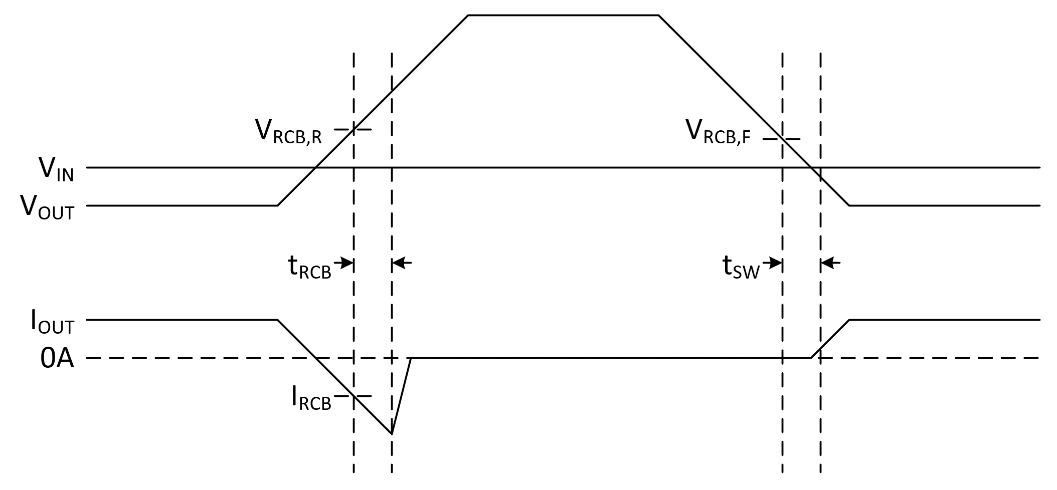
The TPS2117 initiates reverse current blocking (RCB) when the VOUT voltage is externally biased and exceeds the input voltage supply being used. Once the output voltage is higher than the input voltage by 42 mV (VRCB,R), the device will shutoff. During this state, the leakage into VOUT and out of VIN is defined by IREV. Once the voltage difference between the output and input lowers to 17 mV (VRCB,F), the channel will turn back on.
 Figure 7-3 Reverse Current Blocking
Behavior
Figure 7-3 Reverse Current Blocking
BehaviorIf RCB is expected to occur, it is recommended to clamp the output or use a high output capacitance (about 100 µF). This will prevent voltage spikes from damaging the device due to output inductance. Reverse current is not a concern during normal switchover from one channel to another. This is because the device implements a break-before-make switching methodology that prevents cross conduction and will not complete switchover until the output voltage is less than the chosen input voltage.