SLVSGZ5A march   2023  – august 2023 TPS2117

PRODUCTION DATA  

  1.   1
  2. Features
  3. Applications
  4. Description
  5. Revision History
  6. Pin Configuration and Functions
  7. Specifications
    1. 6.1 Absolute Maximum Ratings
    2. 6.2 ESD Ratings
    3. 6.3 Recommended Operating Conditions
    4. 6.4 Thermal Information
    5. 6.5 Electrical Characteristics
    6. 6.6 Switching Characteristics
    7. 6.7 Timing Diagrams
    8. 6.8 Typical Characteristics
  8. Detailed Description
    1. 7.1 Overview
    2. 7.2 Functional Block Diagram
    3. 7.3 Device Functional Modes
      1. 7.3.1 Priority and Manual Mode
        1. 7.3.1.1 Priority Switching
        2. 7.3.1.2 Manual Switching
      2. 7.3.2 Diode Mode
    4. 7.4 Feature Description
      1. 7.4.1 Truth Table
      2. 7.4.2 Soft Start
      3. 7.4.3 Status Indication
      4. 7.4.4 Reverse Current Blocking
    5. 7.5 VINx Collapse Rate
    6. 7.6 Fast Switchover Behavior
    7. 7.7 Output Voltage Drop
  9. Application and Implementation
    1. 8.1 Application Information
    2. 8.2 Typical Application
      1. 8.2.1 Design Requirements
      2. 8.2.2 Detailed Design Procedure
      3. 8.2.3 Application Curves
    3. 8.3 Power Supply Recommendations
    4. 8.4 Layout
      1. 8.4.1 Layout Guidelines
      2. 8.4.2 Layout Example
  10. Device and Documentation Support
    1. 9.1 Documentation Support
      1. 9.1.1 Related Documentation
    2. 9.2 Receiving Notification of Documentation Updates
    3. 9.3 Trademarks
    4. 9.4 Electrostatic Discharge Caution
    5. 9.5 Glossary
  11. 10Mechanical, Packaging, and Orderable Information

Package Options

Mechanical Data (Package|Pins)
Thermal pad, mechanical data (Package|Pins)
Orderable Information

Application Curves

Figure 8-2 shows 5 V being applied to VIN1. The output comes up with slew rate control and limits the inrush current to below 500 mA.
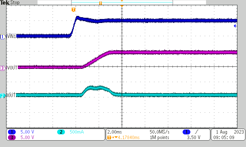
GUID-20230801-SS0I-QB2J-7GPM-RRCHXMMWV5DD-low.png Figure 8-2 TPS2117 Inrush Current Control