SLVSFL4 June 2020 TPS2124
PRODUCTION DATA.
- 1 Features
- 2 Applications
- 3 Description
- 4 Revision History
- 5 Pin Configuration and Functions
- 6 Specifications
- 7 Parameter Measurement Information
-
8 Detailed Description
- 8.1 Overview
- 8.2 Functional Block Diagram
- 8.3 Feature Description
- 8.4 TPS2124 Device Functional Modes
- 9 Application and Implementation
- 10Power Supply Recommendations
- 11Layout
- 12Device and Documentation Support
- 13Mechanical, Packaging, and Orderable Information
Package Options
Mechanical Data (Package|Pins)
- YFP|20
Thermal pad, mechanical data (Package|Pins)
Orderable Information
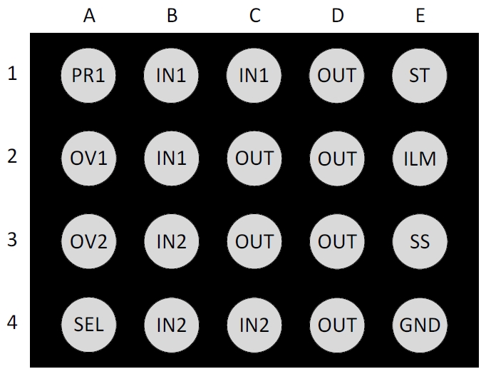
5 Pin Configuration and Functions
TPS2124 (YFP) Package
20-Pin WCSP
Bottom View

Pin Functions
| PIN | I/O | DESCRIPTION | |
|---|---|---|---|
| NAME | TPS2124 | ||
| WCSP | |||
| IN1 | B1, B2, C1 | I | Power Input for Source 1 |
| IN2 | B3, B4, C4 | I | Power Input for Source 2 |
| OUT | C2, C3, D1, D2, D3, D4 | I | Power Output |
| ST | E1 | O | Status output indicating which channel is selected. Connect to GND if not required. |
| ILIM | E2 | O | Output Current Limiting for both channels. |
| SS | E3 | O | Adjusts Input Setting Delay Time and Output Soft Start Time |
| GND | E4 | — | Device Ground |
| PR1 | A1 | I | Enables Priority Operation. Connect to IN1 to set switchover voltage. Connect to GND if not required. |
| OV1 | A2 | I | Active Low Enable Supervisor for IN1 Overvoltage Protection. Connect to GND if not required. |
| OV2 | A3 | I | Active Low Enable Supervisor for IN2 Overvoltage Protection. Connect to GND if not required. |
| SEL | A4 | I | Active low Enable for IN1. Allows GPIO to override priority operation and manually select IN2. |