SLVSDH0C December   2016  – January 2018 TPS22810

PRODUCTION DATA.  

  1. Features
  2. Applications
  3. Description
    1.     Simplified Schematic
  4. Revision History
  5. Device Comparison Table
  6. Pin Configuration and Functions
    1.     Pin Functions
  7. Specifications
    1. 7.1 Absolute Maximum Ratings
    2. 7.2 ESD Ratings
    3. 7.3 Recommended Operating Conditions
    4. 7.4 Thermal Information
    5. 7.5 Electrical Characteristics
    6. 7.6 Switching Characteristics
    7. 7.7 Typical DC Characteristics
    8. 7.8 Typical AC Characteristics
  8. Parameter Measurement Information
  9. Detailed Description
    1. 9.1 Overview
    2. 9.2 Functional Block Diagram
    3. 9.3 Feature Description
      1. 9.3.1 On and Off Control
      2. 9.3.2 Quick Output Discharge (QOD)
        1. 9.3.2.1 QOD when System Power is Removed
        2. 9.3.2.2 Internal QOD Considerations
      3. 9.3.3 EN/UVLO
      4. 9.3.4 Adjustable Rise Time (CT)
      5. 9.3.5 Thermal Shutdown
    4. 9.4 Device Functional Modes
  10. 10Application and Implementation
    1. 10.1 Application Information
    2. 10.2 ON and OFF Control
    3. 10.3 Input Capacitor (Optional)
    4. 10.4 Output Capacitor (Optional)
    5. 10.5 Typical Application
      1. 10.5.1 Design Requirements
      2. 10.5.2 Detailed Design Procedure
        1. 10.5.2.1 Shutdown Sequencing During Unexpected Power Loss
        2. 10.5.2.2 VIN to VOUT Voltage Drop
        3. 10.5.2.3 Inrush Current
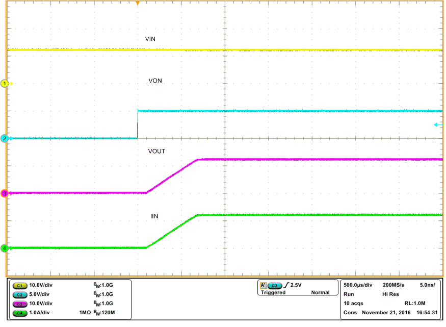
      3. 10.5.3 Application Curves
  11. 11Power Supply Recommendations
  12. 12Layout
    1. 12.1 Layout Guidelines
    2. 12.2 Layout Example
    3. 12.3 Thermal Considerations
  13. 13Device and Documentation Support
    1. 13.1 Device Support
      1. 13.1.1 Developmental Support
    2. 13.2 Documentation Support
      1. 13.2.1 Related Documentation
    3. 13.3 Receiving Notification of Documentation Updates
    4. 13.4 Community Resources
    5. 13.5 Trademarks
    6. 13.6 Electrostatic Discharge Caution
    7. 13.7 Glossary
  14. 14Mechanical, Packaging, and Orderable Information

Package Options

Mechanical Data (Package|Pins)
Thermal pad, mechanical data (Package|Pins)
Orderable Information

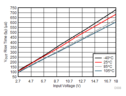
Typical AC Characteristics

TPS22810 D008_SLVSDH0.gif
CIN = 1 µF RL = 10 Ω CL = 0.1 µF
CT = 2200 pF
Figure 7. VOUT Rise Time (tR) vs Input Voltage
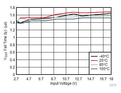
TPS22810 D010_SLVSDH0.gif
CIN = 1 µF RL = 10 Ω CL = 0.1 µF
Figure 9. VOUT Fall Time (tF) vs Input Voltage
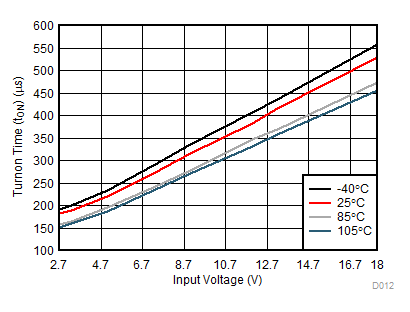
TPS22810 D012_SLVSDH0.gif
CIN = 1 µF RL = 10 Ω CL = 0.1 µF
CT = 2200 pF
Figure 11. Turnon Time (tON) vs Input Voltage
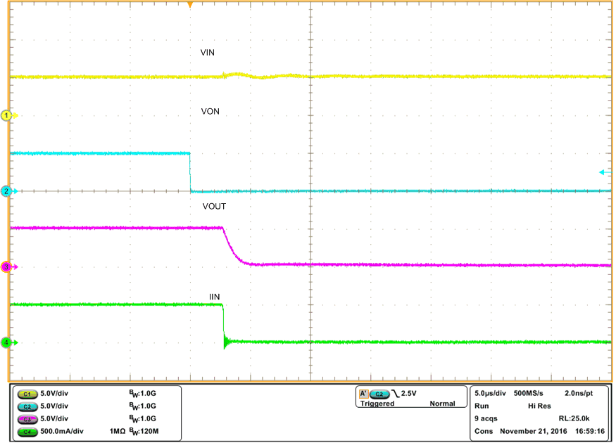
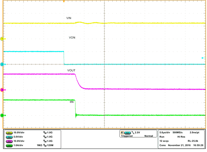
TPS22810 tps22810_Fig16_FallTimeatVIN_5v_CT_.gif
VIN = 5 V CIN = 1 µF CL = 0.1 µF
RL = 10 Ω QOD = Open
Figure 13. Fall Time tF at VIN = 5 V
TPS22810 tps22810_Fig18_FallTimeatVIN_12V_VO.gif
VIN = 12 V CIN = 1 µF CL = 0.1 µF
RL = 10 Ω QOD = Open
Figure 15. Fall Time tF at VIN = 12 V
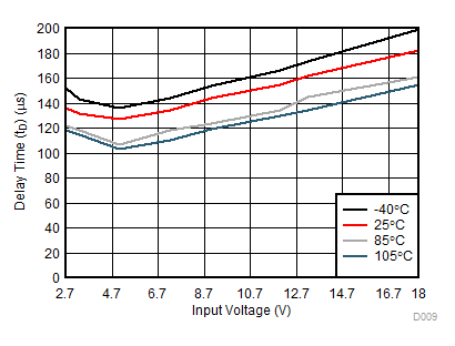
TPS22810 D009_SLVSDH0.gif
CIN = 1 µF RL = 10 Ω CL = 0.1 µF
CT = 2200 pF
Figure 8. Delay Time (tD) vs Input Voltage
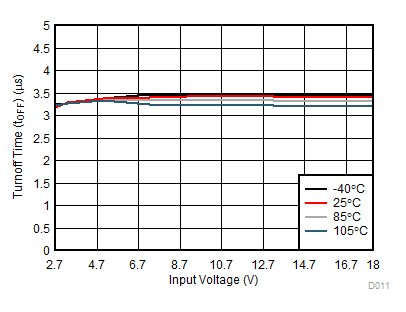
TPS22810 D011_SLVSDH0.gif
CIN = 1 µF RL = 10 Ω CL = 0.1 µF
Figure 10. Turnoff Time (tOFF) vs Input Voltage
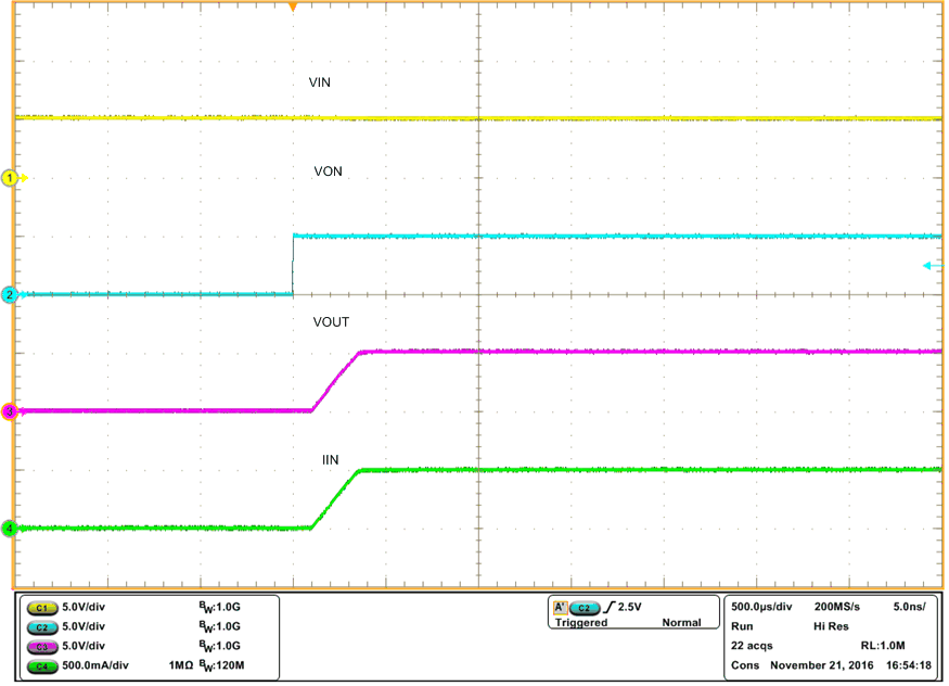
TPS22810 tps22810_Fig15_risetimeatVin5VCT_22.gif
VIN = 5 V CIN = 1 µF CL = 0.1 µF
RL = 10 Ω CT = 2200 pF
Figure 12. Rise Time tR at VIN = 5 V
TPS22810 tps22810_Fig17_RiseTimeatVin12V_CT2.gif
VIN = 12 V CIN = 1 µF CL = 0.1 µF
RL = 10 Ω CT = 2200 pF
Figure 14. Rise Time tR at VIN = 12 V