SLVS827D February   2009  – June 2015 TPS22904

PRODUCTION DATA.  

  1. Features
  2. Applications
  3. Description
  4. Revision History
  5. Device Comparison Table
  6. Pin Configuration and Functions
  7. Specifications
    1. 7.1 Absolute Maximum Ratings
    2. 7.2 ESD Ratings
    3. 7.3 Recommended Operating Conditions
    4. 7.4 Thermal Information
    5. 7.5 Electrical Characteristics
    6. 7.6 Switching Characteristics
    7. 7.7 Typical Characteristics
  8. Parameter Measurement Information
  9. Detailed Description
    1. 9.1 Overview
    2. 9.2 Functional Block Diagram
    3. 9.3 Feature Description
      1. 9.3.1 ON/OFF Control
    4. 9.4 Device Functional Modes
  10. 10Application and Implementation
    1. 10.1 Application Information
      1. 10.1.1 Input Capacitor (Optional)
      2. 10.1.2 Output Capacitor (Optional)
    2. 10.2 Typical Application
      1. 10.2.1 Design Requirements
      2. 10.2.2 Detailed Design Procedure
        1. 10.2.2.1 VIN to VOUT Voltage Drop
      3. 10.2.3 Application Curve
  11. 11Power Supply Recommendations
  12. 12Layout
    1. 12.1 Layout Guidelines
    2. 12.2 Layout Example
  13. 13Device and Documentation Support
    1. 13.1 Related Links
    2. 13.2 Community Resources
    3. 13.3 Trademarks
    4. 13.4 Electrostatic Discharge Caution
    5. 13.5 Glossary
  14. 14Mechanical, Packaging, and Orderable Information

Package Options

Mechanical Data (Package|Pins)
Thermal pad, mechanical data (Package|Pins)
Orderable Information

8 Parameter Measurement Information
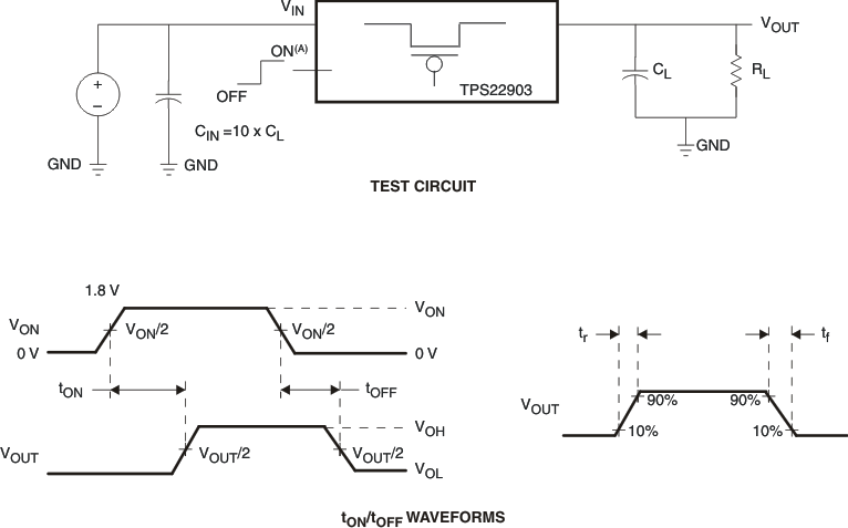
TPS22903 TPS22904 pmi1_lvs827.gif
A. trise and tfall of the control signal is 100 ns.
Figure 27. Test Circuit and tON/tOFF Waveforms