SLVS921A March 2009 – July 2015 TPS22906
PRODUCTION DATA.
- 1 Features
- 2 Applications
- 3 Description
- 4 Revision History
- 5 Device Options
- 6 Pin Configuration and Functions
-
7 Specifications
- 7.1 Absolute Maximum Ratings
- 7.2 ESD Ratings
- 7.3 Recommended Operating Conditions
- 7.4 Thermal Information
- 7.5 Electrical Characteristics
- 7.6 Switching Characteristics - VIN = 1.1 V
- 7.7 Switching Characteristics - VIN = 1.2 V
- 7.8 Switching Characteristics - VIN = 1.8 V
- 7.9 Switching Characteristics - VIN = 2.5 V
- 7.10 Switching Characteristics - VIN = 3 V
- 7.11 Switching Characteristics - VIN = 3.6 V
- 7.12 Typical Characteristics
- 8 Parameter Measurement Information
- 9 Detailed Description
- 10Application and Implementation
- 11Power Supply Recommendations
- 12Layout
- 13Device and Documentation Support
- 14Mechanical, Packaging, and Orderable Information
Package Options
Mechanical Data (Package|Pins)
- YZV|4
Thermal pad, mechanical data (Package|Pins)
Orderable Information
9 Detailed Description
9.1 Overview
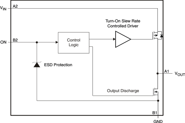
TPS22906 is a low ON-state resistance (rON) load switch with controlled turnon. The device contains a P-channel MOSFET that operates over an input voltage range of 1.0 V to 3.6 V. The switch is controlled by an on/off input (ON), which is capable of interfacing directly with low-voltage control signals. A 120-Ω on-chip load resistor is added for output quick discharge when the switch is turned off.
9.2 Functional Block Diagram

9.3 Feature Description
9.3.1 ON/OFF Control
The ON pin controls the state of the switch. Activating ON continuously holds the switch in the on state so long as there is no fault. ON is active HI and has a low threshold making it capable of interfacing with low-voltage signals. The ON pin is compatible with standard GPIO logic threshold. It can be used with any microcontroller with 1.2-V, 1.8-V, 2.5-V, or 3.3-V GPIOs.
9.4 Device Functional Modes
Table 1 lists the functional modes of the TPS22906.
Table 1. Function Table
| ON (CONTROL INPUT) | VIN TO VOUT | VOUT TO GND |
|---|---|---|
| L | OFF | ON |
| H | ON | OFF |