SLVSBI7C July   2012  – April 2015 TPS22908

PRODUCTION DATA.  

  1. Features
  2. Applications
  3. Description
  4. Revision History
  5. Device Options
  6. Pin Configuration and Functions
  7. Specifications
    1. 7.1 Absolute Maximum Ratings
    2. 7.2 ESD Ratings
    3. 7.3 Recommended Operating Conditions
    4. 7.4 Thermal Information
    5. 7.5 Electrical Characteristics
    6. 7.6 Switching Characteristics
    7. 7.7 Typical Characteristics
      1. 7.7.1 Typical DC Characteristics
      2. 7.7.2 Typical Switching Characteristics
  8. Parameter Measurement Information
  9. Detailed Description
    1. 9.1 Overview
    2. 9.2 Functional Block Diagram
    3. 9.3 Feature Description
      1. 9.3.1 ON/OFF Control
      2. 9.3.2 Quick Output Discharge
    4. 9.4 Device Functional Modes
  10. 10Application and Implementation
    1. 10.1 Application Information
      1. 10.1.1 Input Capacitor (Optional)
      2. 10.1.2 Output Capacitor (Optional)
    2. 10.2 Typical Application
      1. 10.2.1 Design Requirements
      2. 10.2.2 Detailed Design Procedure
        1. 10.2.2.1 Managing Inrush Current
        2. 10.2.2.2 VIN to VOUT Voltage Drop
      3. 10.2.3 Application Curve
  11. 11Power Supply Recommendations
  12. 12Layout
    1. 12.1 Layout Guidelines
    2. 12.2 Layout Example
    3. 12.3 Thermal Considerations
  13. 13Device and Documentation Support
    1. 13.1 Trademarks
    2. 13.2 Electrostatic Discharge Caution
    3. 13.3 Glossary
  14. 14Mechanical, Packaging, and Orderable Information

Package Options

Mechanical Data (Package|Pins)
Thermal pad, mechanical data (Package|Pins)
Orderable Information

6 Pin Configuration and Functions

YZT PACKAGE
4-PIN DSBGA
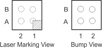
TPS22908 po_lvsbi7.gif

Pin Functions

PIN I/O DESCRIPTION
NO. NAME
A1 VOUT O Switch Output
A2 VIN I Switch input, bypass capacitor recommended for minimizing VIN dip. See Application Information.
B1 GND Ground
B2 ON I Switch control input, active high. Do not leave floating.