SLVSD76C February   2016  – July 2017 TPS22918

PRODUCTION DATA.  

  1. Features
  2. Applications
  3. Description
  4. Revision History
  5. Pin Configuration and Functions
  6. Specifications
    1. 6.1 Absolute Maximum Ratings
    2. 6.2 ESD Ratings
    3. 6.3 Recommended Operating Conditions
    4. 6.4 Thermal Information
    5. 6.5 Electrical Characteristics
    6. 6.6 Switching Characteristics
    7. 6.7 Typical DC Characteristics
    8. 6.8 Typical AC Characteristics
  7. Parameter Measurement Information
  8. Detailed Description
    1. 8.1 Overview
    2. 8.2 Functional Block Diagram
    3. 8.3 Feature Description
      1. 8.3.1 On and Off Control
      2. 8.3.2 Quick Output Discharge (QOD)
        1. 8.3.2.1 QOD when System Power is Removed
        2. 8.3.2.2 Internal QOD Considerations
      3. 8.3.3 Adjustable Rise Time (CT)
    4. 8.4 Device Functional Modes
  9. Application and Implementation
    1. 9.1 Application Information
    2. 9.2 Typical Application
      1. 9.2.1 Design Requirements
      2. 9.2.2 Detailed Design Procedure
        1. 9.2.2.1 Input Capacitor (CIN)
        2. 9.2.2.2 Output Capacitor (CL) (Optional)
        3. 9.2.2.3 Shutdown Sequencing During Unexpected System Power Loss
        4. 9.2.2.4 VIN to VOUT Voltage Drop
        5. 9.2.2.5 Inrush Current
      3. 9.2.3 Application Curves
  10. 10Power Supply Recommendations
  11. 11Layout
    1. 11.1 Layout Guidelines
    2. 11.2 Layout Example
    3. 11.3 Thermal Considerations
  12. 12Device and Documentation Support
    1. 12.1 Device Support
      1. 12.1.1 Developmental Support
    2. 12.2 Documentation Support
      1. 12.2.1 Related Documentation
    3. 12.3 Community Resources
    4. 12.4 Trademarks
    5. 12.5 Electrostatic Discharge Caution
    6. 12.6 Glossary
  13. 13Mechanical, Packaging, and Orderable Information

Package Options

Mechanical Data (Package|Pins)
Thermal pad, mechanical data (Package|Pins)
Orderable Information

Parameter Measurement Information

TPS22918 section_81.png
Rise and fall times of the control signal are 100 ns
Turn-off times and fall times are dependent on the time constant at the load. For TPS22918, the internal pull-down resistance RPD is enabled when the switch is disabled. The time constant is (RQOD || RL) × CL.
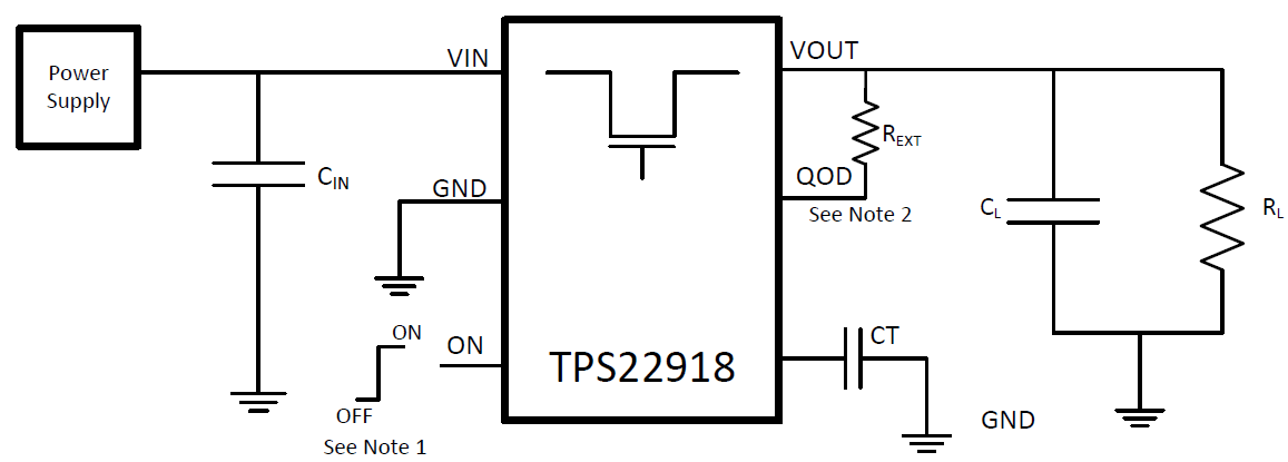
Figure 21. Test Circuit
TPS22918 time_wave_slvsco0.gif Figure 22. Timing Waveforms