SLVSBT4A May 2013 – August 2015 TPS22924D
PRODUCTION DATA.
- 1 Features
- 2 Applications
- 3 Description
- 4 Revision History
- 5 Pin Configuration and Functions
- 6 Specifications
- 7 Parametric Measurement Information
- 8 Detailed Description
- 9 Application and Implementation
- 10Power Supply Recommendations
- 11Layout
- 12Device and Documentation Support
- 13Mechanical, Packaging, and Orderable Information
Package Options
Mechanical Data (Package|Pins)
- YZP|6
Thermal pad, mechanical data (Package|Pins)
Orderable Information
8 Detailed Description
8.1 Overview
The TPS22924D is a single channel, 2-A load switch in a small, space-saving CSP-6 package. This device implements a low resistance N-channel MOSFET with a controlled rise time for applications that need to limit the inrush current.
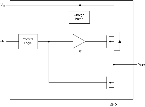
This device is also designed to have very low leakage current during off state. This prevents downstream circuits from pulling high standby current from the supply. Integrated control logic, driver, power supply, and output discharge FET eliminates the need for additional external components, which reduces solution size and bill of materials (BOM) count.
8.2 Functional Block Diagram

8.3 Feature Description
Table 1 lists the features of the TPS2222924D device.
Table 1. Feature List
| DEVICE | rON (TYP) AT 3.6 V |
SLEW RATE (TYP) AT 3.6 V |
QUICK OUTPUT DISCHARGE (1) | MAXIMUM OUTPUT CURRENT | ENABLE |
|---|---|---|---|---|---|
| TPS22924D | 18.3 mΩ | 6200 μs | Yes | 2 A | Active high |
8.3.1 ON/OFF Control
The ON pin controls the state of the switch. Asserting ON high enables the switch. ON is active high and has a low threshold, making it capable of interfacing with low-voltage signals. The ON pin is compatible with standard GPIO logic threshold. It can be used with any microcontroller with 1.2-V, 1.8-V, 2.5-V or 3.3-V GPIOs.
8.3.2 Output Pulldown
The output pulldown is active when the user is turning off the main pass FET. The pulldown discharges the output rail to approximately 10% of the rail, then the output pulldown is automatically disconnected to optimize the shutdown current.
8.4 Device Functional Modes
Table 2 lists the functional modes of the TPS22924D device.
Table 2. Function Table
| ON (Control Signal) | VIN to VOUT | VOUT to GND (1) |
|---|---|---|
| L | OFF | ON |
| H | ON | OFF |