SLVS840D November   2015  – August 2016 TPS22925

PRODUCTION DATA.  

  1. Features
  2. Applications
  3. Description
  4. Revision History
  5. Device Comparison Table
  6. Pin Configuration and Functions
  7. Specifications
    1. 7.1 Absolute Maximum Ratings
    2. 7.2 ESD Ratings
    3. 7.3 Recommended Operating Conditions
    4. 7.4 Thermal Information
    5. 7.5 Electrical Characteristics
    6. 7.6 Switching Characteristics
    7. 7.7 Typical Characteristics
    8. 7.8 Typical Characteristics
  8. Detailed Description
    1. 8.1 Overview
    2. 8.2 Functional Block Diagram
    3. 8.3 Feature Description
      1. 8.3.1 ON and OFF Control
      2. 8.3.2 Quick Output Discharge (QOD) (TPS22925B and TPS22925C Only)
      3. 8.3.3 Reverse Current Blocking
    4. 8.4 Device Functional Modes
  9. Application and Implementation
    1. 9.1 Application Information
      1. 9.1.1 VIN to VOUT Voltage Drop
      2. 9.1.2 Input Capacitor (CIN)
      3. 9.1.3 Load Capacitor (CL)
      4. 9.1.4 Standby Power Reduction
      5. 9.1.5 Power Multiplexing
      6. 9.1.6 Thermal Considerations
    2. 9.2 Typical Application
      1. 9.2.1 Design Requirements
      2. 9.2.2 Detailed Design Procedure
        1. 9.2.2.1 Managing Inrush Current
      3. 9.2.3 Application Curve
  10. 10Power Supply Recommendations
  11. 11Layout
    1. 11.1 Layout Guidelines
    2. 11.2 Layout Example
  12. 12Device and Documentation Support
    1. 12.1 Documentation Support
      1. 12.1.1 Related Documentation
    2. 12.2 Receiving Notification of Documentation Updates
    3. 12.3 Community Resources
    4. 12.4 Trademarks
    5. 12.5 Electrostatic Discharge Caution
    6. 12.6 Glossary
  13. 13Mechanical, Packaging, and Orderable Information

Package Options

Mechanical Data (Package|Pins)
Thermal pad, mechanical data (Package|Pins)
Orderable Information

11 Layout

11.1 Layout Guidelines

For best performance, all traces must be as short as possible. To be most effective, the input and load capacitors must be placed close to the device to minimize the effects that parasitic trace inductances may have on operation. Using wide traces for VIN, VOUT, and GND helps minimize the parasitic electrical effects.

11.2 Layout Example
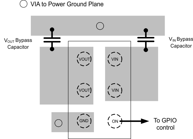
TPS22925 layout_slvs840.gif Figure 35. TPS22925xx Layout Example