SLVS802C August 2009 – May 2015 TPS22932B
PRODUCTION DATA.
- 1 Features
- 2 Applications
- 3 Description
- 4 Revision History
- 5 Device Comparison Table
- 6 Pin Configuration and Functions
-
7 Specifications
- 7.1 Absolute Maximum Ratings
- 7.2 ESD Ratings
- 7.3 Recommended Operating Conditions
- 7.4 Thermal Information
- 7.5 Electrical Characteristics
- 7.6 Switching Characteristics, 1.2 V
- 7.7 Switching Characteristics, 1.5 V
- 7.8 Switching Characteristics, 1.8 V
- 7.9 Switching Characteristics, 2.5 V
- 7.10 Switching Characteristics, 3 V
- 7.11 Switching Characteristics, 3.3 V
- 7.12 Typical Characteristics
- 8 Parameter Measurement information
- 9 Detailed Description
- 10Application and Implementation
- 11Power Supply Recommendations
- 12Layout
- 13Device and Documentation Support
- 14Mechanical, Packaging, and Orderable Information
Package Options
Mechanical Data (Package|Pins)
- YFP|6
Thermal pad, mechanical data (Package|Pins)
Orderable Information
9 Detailed Description
9.1 Overview
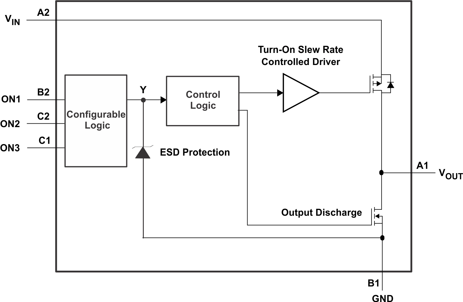
TPS22932B is a single-channel, low rON load switch with controlled turnon. The device contains a low rON P-channel MOSFET that can operate over an input voltage range of 1.1 V to 3.6 V. The switch is controlled by eight patterns of 3-bit input. The user can choose the logic functions MUX, AND, OR, NAND, NOR, inverter, and noninverter. All inputs can be connected to VIN or GND. The control pins can be connected to low-voltage GPIOs allowing it to be controlled by either 1.2-V, 1.8-V, 2.5-V, or 3.3-V logic signals while keeping extremely low quiescent current. A 120-Ω on-chip load resistor is available for output quick discharge when the switch is turned off. The rise time (slew rate) of the device is internally controlled to avoid inrush current.
9.2 Functional Block Diagram
9.3 Feature Description
9.3.1 Configurable Logic Function
The switch is controlled by eight patterns of 3-bit input. The user can choose the logic functions MUX, AND, OR, NAND, NOR, inverter, and noninverter. All inputs can be connected to VIN or GND. The control pins can be connected to low-voltage GPIOs allowing it to be controlled by either 1.2-V, 1.8-V, 2.5-V, or 3.3-V logic signals while keeping extremely low quiescent current.
9.3.2 Quick Output Discharge
The TPS22932B includes the Quick Output Discharge (QOD) feature. When the switch is disabled, a discharge resistance with a typical value of 120 Ω is connected between the output and ground. This resistance pulls down the output and prevents it from floating when the device is disabled.
9.4 Device Functional Modes
9.4.1 Logic Configurations
Table 1. Configurable Logic Function Table
| INPUTS | SWITCH CONTROL | |||
|---|---|---|---|---|
| ON3 | ON2 | ON1 | Y | |
| L | L | L | OFF | |
| L | L | H | OFF | |
| L | H | L | ON | |
| L | H | H | ON | |
| H | L | L | OFF | |
| H | L | H | ON | |
| H | H | L | OFF | |
| H | H | H | ON | |
 Figure 31. Logic Diagram (Positive Logic)
Table 2. Function Selection Table
| LOGIC FUNCTION | FIGURE NO. | |||
|---|---|---|---|---|
| 2-to-1 data selector | Figure 32 | |||
| 2-input AND gate | Figure 33 | |||
| 2-input OR gate with one inverted input | Figure 34 | |||
| 2-input NAND gate with one inverted input | Figure 34 | |||
| 2-input AND gate with one inverted input | Figure 35 | |||
| 2-input NOR gate with one inverted input | Figure 35 | |||
| 2-input OR gate | Figure 36 | |||
| Inverter | Figure 37 | |||
| Noninverted buffer | Figure 38 | |||
 Figure 32. 2-to-1 Data Selector
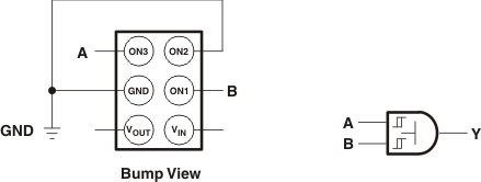 Figure 33. 2-Input AND Gate
 Figure 34. 2-Input OR Gate With One Inverted Input, 2-Input NAND Gate With One Inverted Input
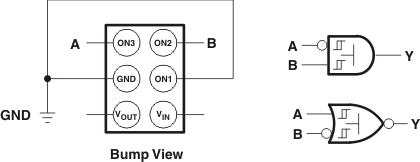 Figure 35. 2-Input AND Gate With One Inverted Input, 2-Input NOR Gate With One Inverted Input
 Figure 36. 2-Input OR Gate
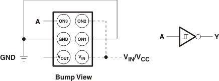 Figure 37. Inverter
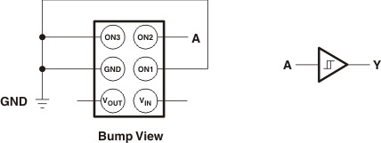 Figure 38. Noninverted Buffer