SLVS984B September 2009 – March 2015 TPS22946
PRODUCTION DATA.
- 1 Features
- 2 Applications
- 3 Description
- 4 Revision History
- 5 Pin Configuration and Functions
- 6 Specifications
- 7 Parameter Measurement Information
- 8 Detailed Description
- 9 Application and Implementation
- 10Power Supply Recommendations
- 11Layout
- 12Device and Documentation Support
- 13Mechanical, Packaging, and Orderable Information
Package Options
Mechanical Data (Package|Pins)
- YZP|6
Thermal pad, mechanical data (Package|Pins)
Orderable Information
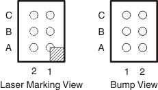
5 Pin Configuration and Functions
6-Pin DSBGA
YZP Package

Pin Assignments
| C | ON | OC |
| B | CL | GND |
| A | VIN | VOUT |
| 2 | 1 |
Pin Functions
| PIN | I/O | DESCRIPTION | |
|---|---|---|---|
| NO. | NAME | ||
| A1 | VOUT | O | Output of the power switch |
| A2 | VIN | I | Supply. Input to the power switch and the supply voltage for the device |
| B1 | GND | – | Ground |
| B2 | CL | I | Current limit selection. CL high is 155-mA current limit, CL low is 70-mA current limit, and CL floating is 30-mA current limit. |
| C1 | OC | O | Overcurrent output flag. Active-low open-drain output that indicates an overcurrent, supply undervoltage, or overtemperature state. |
| C2 | ON | I | On/off control input |