SLVSFJ2B December   2020  – February 2023 TPS22950

PRODUCTION DATA  

  1. Features
  2. Application
  3. Description
  4. Revision History
  5. Device Comparison Table
  6. Pin Configuration and Functions
  7. Specifications
    1. 7.1 Absolute Maximum Ratings
    2. 7.2 ESD Ratings
    3. 7.3 Recommended Operating Conditions
    4. 7.4 Thermal Information
    5. 7.5 Electrical Characteristics
    6. 7.6 Switching Characteristics
    7. 7.7 Typical Characteristics
  8. Parameter Measurement Information
  9. Detailed Description
    1. 9.1 Overview
    2. 9.2 Functional Block Diagram
    3. 9.3 Feature Description
      1. 9.3.1 Current Limiting (TPS22950, TPS22950C)
      2. 9.3.2 Current Limiting (TPS22950L)
      3. 9.3.3 Adjusting the Current Limit
      4. 9.3.4 Reverse Current Blocking (TPS22950, TPS22950C)
    4. 9.4 Device Functional Modes
  10. 10Application and Implementation
    1. 10.1 Application Information
    2. 10.2 Typical Application
      1. 10.2.1 Design Requirements
      2. 10.2.2 Detailed Design Procedure
      3. 10.2.3 Application Curves
    3. 10.3 Power Supply Recommendations
    4. 10.4 Layout
      1. 10.4.1 Layout Guidelines
      2. 10.4.2 Layout Example
  11. 11Device and Documentation Support
    1. 11.1 Receiving Notification of Documentation Updates
    2. 11.2 Support Resources
    3. 11.3 Trademarks
    4. 11.4 Electrostatic Discharge Caution
    5. 11.5 Glossary
  12. 12Mechanical, Packaging, and Orderable Information

Package Options

Refer to the PDF data sheet for device specific package drawings

Mechanical Data (Package|Pins)
  • YBH|6
  • DDC|6
Thermal pad, mechanical data (Package|Pins)
Orderable Information

Typical Characteristics

GUID-20201210-CA0I-WHSW-JR1G-G92KZDRHSMJZ-low.gif
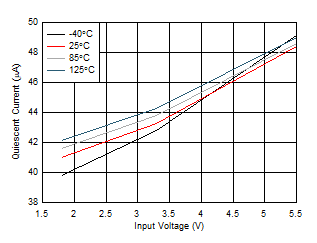
VON ≥ VIH
Figure 7-1 Quiescent Current vs Input Voltage
GUID-20201210-CA0I-MF3C-WHXC-MXTTJM3RQHM1-low.gif
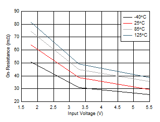
VON ≥ VIH IOUT = –200 mA
Figure 7-3 On-Resistance vs Input Voltage
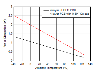
GUID-20201214-CA0I-KNB1-0903-2VDVCM2VBZXH-low.gifFigure 7-5 Maximum Power Dissipation vs Ambient Temperature
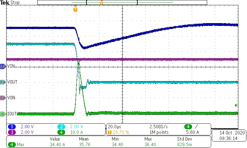
GUID-20201210-CA0I-9GLJ-PFFC-35GCWLGR0GNW-low.jpg
VIN = 5 V VON = 5 V
Figure 7-7 Short-Circuit Response
GUID-20201210-CA0I-DG37-T36F-V9KDQDHTQB6R-low.gif
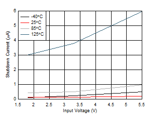
VON ≤ VIL
Figure 7-2 Shutdown Current vs Input Voltage
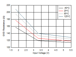
GUID-20201210-CA0I-9DQM-1C58-VVTCKTPHTH7D-low.gif
VON ≤ VIL
Figure 7-4 QOD Resistance vs Input Voltage
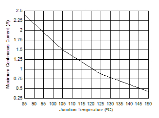
GUID-20201214-CA0I-TC46-69PN-V6QNPKZ91TQB-low.gifFigure 7-6 Maximum Continuous Current vs Junction Temperature
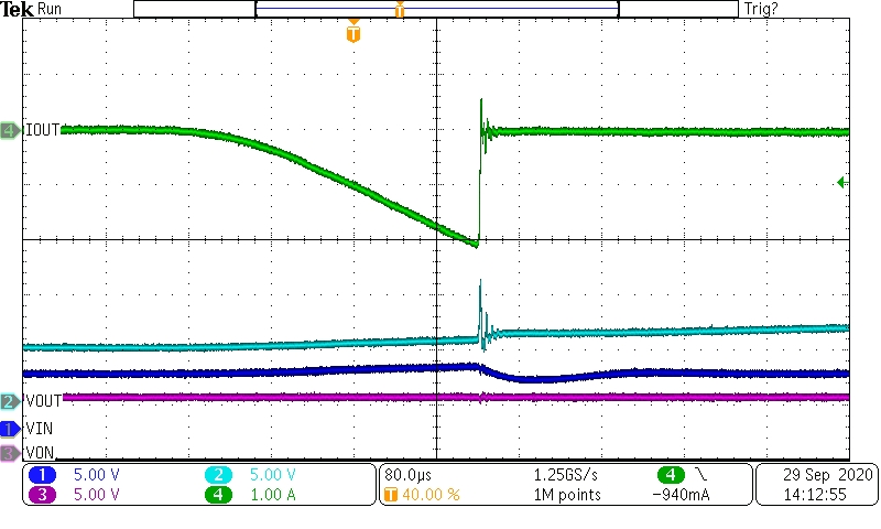
GUID-20201210-CA0I-LXJW-DNKB-DZ2VKHLFJNST-low.jpg
VIN = 5 V VON = 5 V
Figure 7-8 Reverse Current Blocking