SLVSC71B December 2013 – March 2020 TPS22966-Q1
PRODUCTION DATA.
- 1 Features
- 2 Applications
- 3 Description
- 4 Revision History
- 5 Pin Configuration and Functions
- 6 Specifications
- 7 Parameter Measurement Information
- 8 Detailed Description
- 9 Application and Implementation
- 10Power Supply Recommendations
- 11Layout
- 12Device and Documentation Support
- 13Mechanical, Packaging, and Orderable Information
Package Options
Mechanical Data (Package|Pins)
- DPU|14
Thermal pad, mechanical data (Package|Pins)
Orderable Information
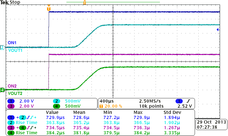
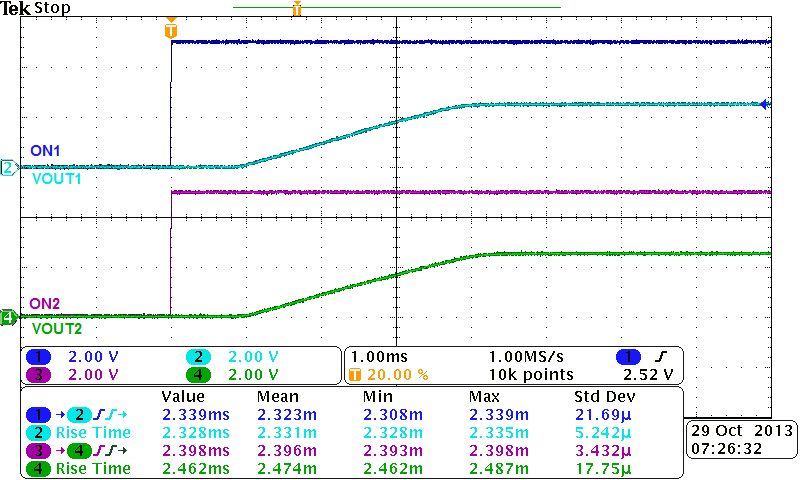
6.8.1 Typical AC Scope Captures at TA = 25ºC, CT = 1 nF
 Figure 23. Turnon Response Time (VIN = 0.8 V, VBIAS = 2.5 V, CIN = 1 µF, CL = 0.1 µF, RL = 10 Ω)
  Figure 24. Turnon Response Time (VIN = 0.8 V, VBIAS = 5 V, CIN = 1 µF, CL = 0.1 µF, RL = 10 Ω)
  Figure 25. Turnon Response Time (VIN = 2.5 V, VBIAS = 2.5 V, CIN = 1 µF, CL = 0.1 µF, RL = 10 Ω)
  Figure 27. Turnoff Response Time (VIN = 0.8 V, VBIAS = 2.5 V, CIN = 1 µF, CL = 0.1 µF, RL = 10 Ω)
  Figure 29. Turnoff Response Time (VIN = 2.5 V, VBIAS = 2.5 V, CIN = 1 µF, CL = 0.1 µF, RL = 10 Ω)
  Figure 26. Turnon Response Time (VIN = 5 V, VBIAS = 5 V, CIN = 1 µF, CL = 0.1 µF, RL = 10 Ω)
  Figure 28. Turnoff Response Time (VIN = 0.8 V, VBIAS = 5 V, CIN = 1 µF, CL = 0.1 µF, RL = 10 Ω)
  Figure 30. Turnoff Response Time (VIN = 5 V, VBIAS = 5 V, CIN = 1 µF, CL = 0.1 µF, RL = 10 Ω)