SLVSCP7B November 2014 – March 2016 TPS22968-Q1
PRODUCTION DATA.
- 1 Features
- 2 Applications
- 3 Description
- 4 Revision History
- 5 Device Comparison Table
- 6 Pin Configuration and Functions
-
7 Specifications
- 7.1 Absolute Maximum Ratings
- 7.2 ESD Ratings
- 7.3 Recommended Operating Conditions
- 7.4 Thermal Information
- 7.5 Electrical Characteristics (VBIAS = 5 V)
- 7.6 Electrical Characteristics (VBIAS = 3.3 V)
- 7.7 Electrical Characteristics (VBIAS = 2.5 V)
- 7.8 Switching Characteristics
- 7.9 Typical Characteristics
- 8 Parameter Measurement Information
- 9 Detailed Description
- 10Application and Implementation
- 11Power Supply Recommendations
- 12Layout
- 13Device and Documentation Support
- 14Mechanical, Packaging, and Orderable Information
Package Options
Mechanical Data (Package|Pins)
- DMG|10
Thermal pad, mechanical data (Package|Pins)
- DMG|10
Orderable Information
12 Layout
12.1 Layout Guidelines
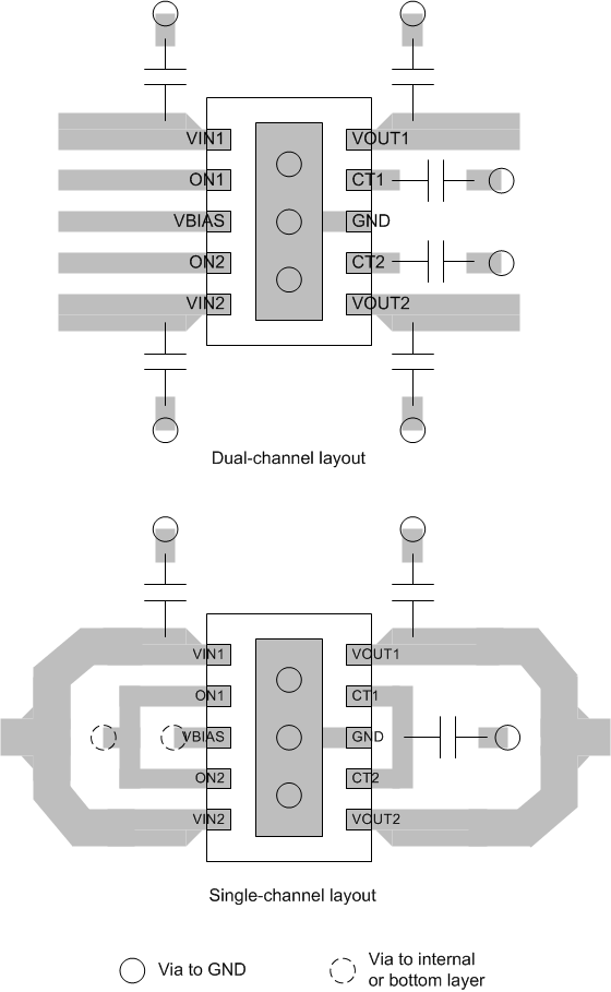
- VIN and VOUT traces should be as short and wide as possible to accommodate for high current.
- Use vias under the exposed thermal pad for thermal relief for high current operation.
- VINx pins should be bypassed to ground with low-ESR ceramic bypass capacitors. The typical recommended bypass capacitance is 1-µF ceramic with X5R or X7R dielectric. This capacitor should be placed as close to the device pins as possible.
- VOUTx pins should be bypassed to ground with low-ESR ceramic bypass capacitors. The typical recommended bypass capacitance is one-tenth of the VINx bypass capacitor of X5R or X7R dielectric rating. This capacitor should be placed as close to the device pins as possible.
- The VBIAS pin should be bypassed to ground with low-ESR ceramic bypass capacitors. The typical recommended bypass capacitance is 0.1-µF ceramic with X5R or X7R dielectric.
- The CTx capacitors should be placed as close to the device pins as possible. The typical recommended CTx capacitance is a capacitor of X5R or X7R dielectric rating with a rating of 25 V or higher.
12.2 Layout Example
 Figure 43. Layout Schematic
12.3 Thermal Considerations
The maximum IC junction temperature should be restricted to 150°C under normal operating conditions. To calculate the maximum allowable dissipation, PD(max) for a given ambient temperature, use Equation 5.

where
- PD(max) = maximum allowable power dissipation
- TJ(max) = maximum allowable junction temperature (150°C for the TPS22968x-Q1)
- TA = ambient temperature of the device
- RθJA = junction to air thermal impedance. See Thermal Information. This parameter is highly dependent upon board layout.
Following are two examples demonstrating how to use the above information: For VBIAS = 5 V, VIN = 5 V, the maximum allowable ambient temperature with a 3-A load through each channel can be determined by using the following calculations.
NOTE
When calculating power dissipation in the switch, it is important to use the correct RON value. RON is dependent on the junction temperature of the device.

For VBIAS = 5 V, VIN = 5 V, the maximum continuous current for an ambient temperature of 85°C with the same current flowing through each channel can be determined by using the following calculation:


