SLVSGT0 December 2022 TPS22997
PRODUCTION DATA
- 1 Features
- 2 Applications
- 3 Description
- 4 Revision History
- 5 Pin Configuration and Functions
-
6 Specifications
- 6.1 Absolute Maximum Ratings
- 6.2 ESD Ratings
- 6.3 Recommended Operating Conditions
- 6.4 Thermal Information
- 6.5 Electrical Characteristics (VBIAS = 5 V)
- 6.6 Electrical Characteristics (VBIAS = 3.3 V)
- 6.7 Electrical Characteristics (VBIAS = 1.5 V)
- 6.8 Switching Characteristics (VBIAS = 5 V)
- 6.9 Switching Characteristics (VBIAS = 3.3 V)
- 6.10 Switching Characteristics (VBIAS = 1.5 V)
- 6.11 Typical Characteristics
- 7 Parameter Measurement Information
- 8 Detailed Description
- 9 Application and Implementation
- 10Device and Documentation Support
- 11Mechanical, Packaging, and Orderable Information
Package Options
Mechanical Data (Package|Pins)
- RYZ|10
Thermal pad, mechanical data (Package|Pins)
Orderable Information
3 Description
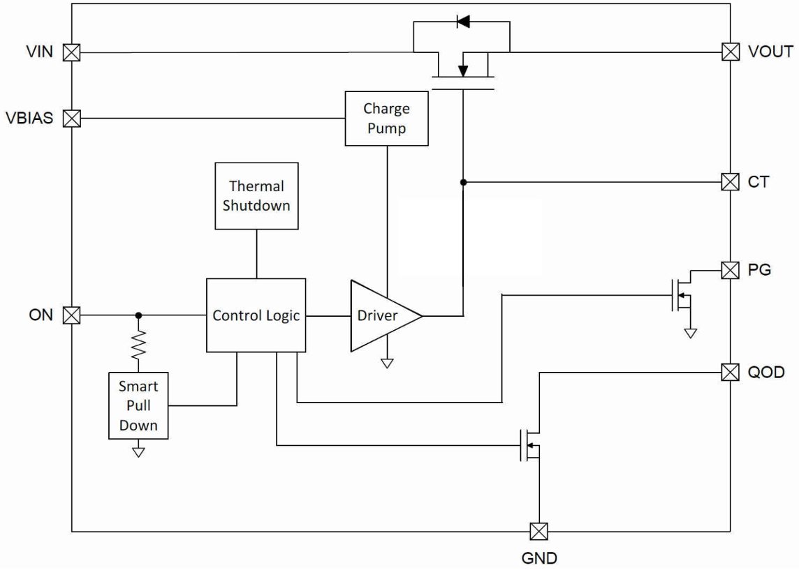
The TPS22997 is a single-channel load switch that provides a configurable rise time to minimize inrush current. The device contains an N-channel MOSFET that can operate over an input voltage range of 0.1 V to 5.5 V and can support a maximum continuous current of 10 A.
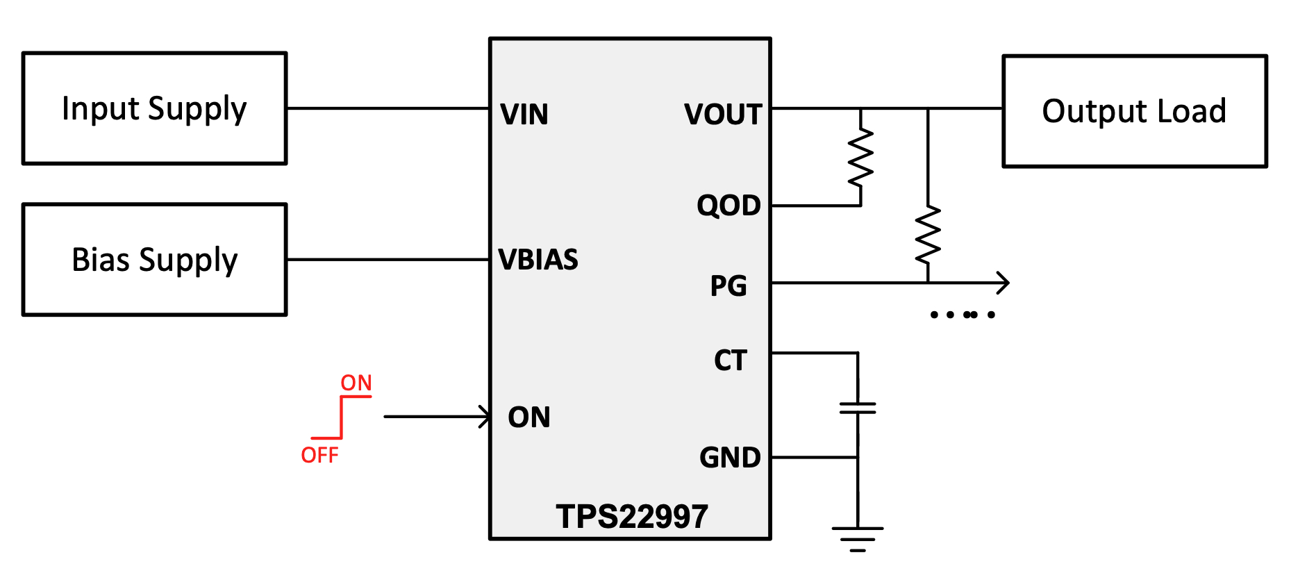
The switch is controlled by an enable pin (ON), which is capable of interfacing directly with low voltage GPIO signals (VIH = 0.8 V). The TPS22997 device has an optional QOD pin for quick output discharge when switch is turned off, and the fall time (tFALL) of the output can be adjusted through an external resistor. There is a Power Good (PG) signal on the device that indicates when the main MOSFET is fully turned on, which can be used to enable a downstream load. Integrated thermal shutdown ensures protection in high temperature environments.
The TPS22997 is available in a 1.5 × 2.0 mm, 0.5 mm pitch, 10-pin WQFN package (RYZ) and is characterized for operation over the free-air temperature range of –40°C to +125°C.
| PART NUMBER | PACKAGE(1) | BODY SIZE (NOM) |
|---|---|---|
TPS22997 | WQFN (10) | 1.5 × 2.0 mm |
 TPS22997 Block Diagram
 TPS22997 Typical Application