SLVSGT0 December 2022 TPS22997
PRODUCTION DATA
- 1 Features
- 2 Applications
- 3 Description
- 4 Revision History
- 5 Pin Configuration and Functions
-
6 Specifications
- 6.1 Absolute Maximum Ratings
- 6.2 ESD Ratings
- 6.3 Recommended Operating Conditions
- 6.4 Thermal Information
- 6.5 Electrical Characteristics (VBIAS = 5 V)
- 6.6 Electrical Characteristics (VBIAS = 3.3 V)
- 6.7 Electrical Characteristics (VBIAS = 1.5 V)
- 6.8 Switching Characteristics (VBIAS = 5 V)
- 6.9 Switching Characteristics (VBIAS = 3.3 V)
- 6.10 Switching Characteristics (VBIAS = 1.5 V)
- 6.11 Typical Characteristics
- 7 Parameter Measurement Information
- 8 Detailed Description
- 9 Application and Implementation
- 10Device and Documentation Support
- 11Mechanical, Packaging, and Orderable Information
Package Options
Mechanical Data (Package|Pins)
- RYZ|10
Thermal pad, mechanical data (Package|Pins)
Orderable Information
5 Pin Configuration and Functions
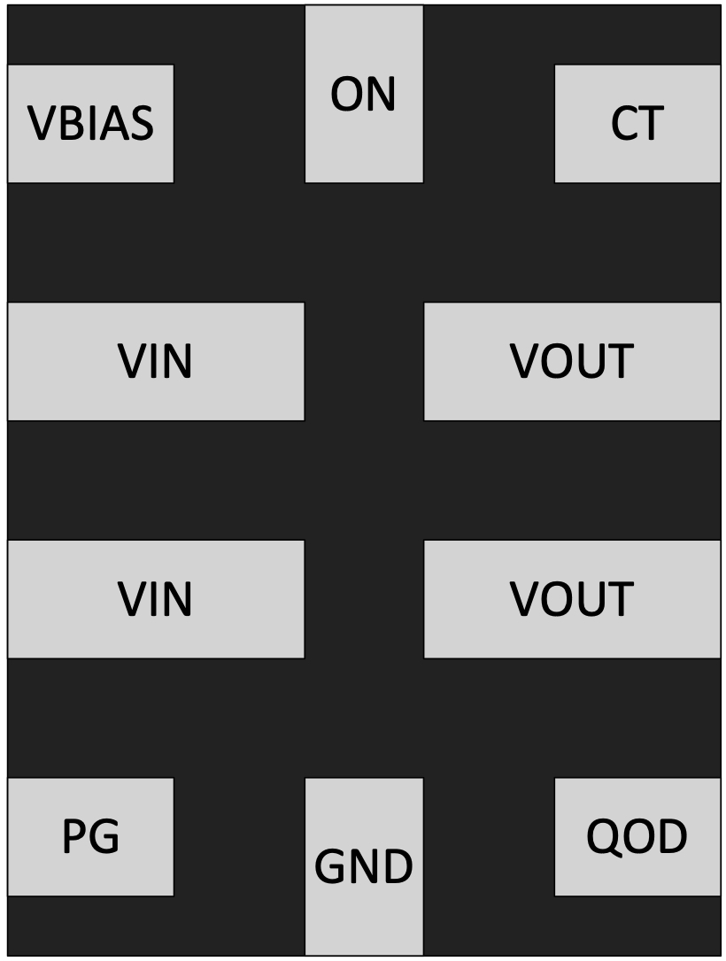
 Figure 5-1 TPS22997 RYZ Package, 10-Pin WQFN (Top View)
Table 5-1 Pin Functions
| PIN | I/O(1) | DESCRIPTION | |
|---|---|---|---|
| NAME | NO. | ||
VBIAS | 1 | I | Device bias supply |
VIN | 2, 3 | I | Switch input |
PG | 4 | O | Open drain power good signal, asserted high when the output is full load ready |
GND | 5 | - | Device ground |
QOD | 6 | - | Quick output discharge pin |
VOUT | 7, 8 | O | Switch output |
CT | 9 | I | Timing pin, can control the slew rate of the output through a capacitor to GND |
ON | 10 | I | Enable pin |
(1) I = Input, O = Output