SLVSG05A October 2021 – December 2021 TPS22998
PRODUCTION DATA
- 1 Features
- 2 Applications
- 3 Description
- 4 Revision History
- 5 Pin Configuration and Functions
-
6 Specifications
- 6.1 Absolute Maximum Ratings
- 6.2 ESD Ratings
- 6.3 Recommended Operating Conditions
- 6.4 Thermal Information
- 6.5 Electrical Characteristics (VBIAS = 5 V)
- 6.6 Electrical Characteristics (VBIAS = 3.3 V)
- 6.7 Electrical Characteristics (VBIAS = 2.2 V)
- 6.8 Switching Characteristics (VBIAS = 2.2 V to 5 V)
- 6.9 Timing Diagram
- 6.10 Typical Characteristics
- 7 Detailed Description
- 8 Application and Implementation
- 9 Power Supply Recommendations
- 10Layout
- 11Device and Documentation Support
- 12Mechanical, Packaging, and Orderable Information
Package Options
Mechanical Data (Package|Pins)
- RYZ|10
Thermal pad, mechanical data (Package|Pins)
Orderable Information
3 Description
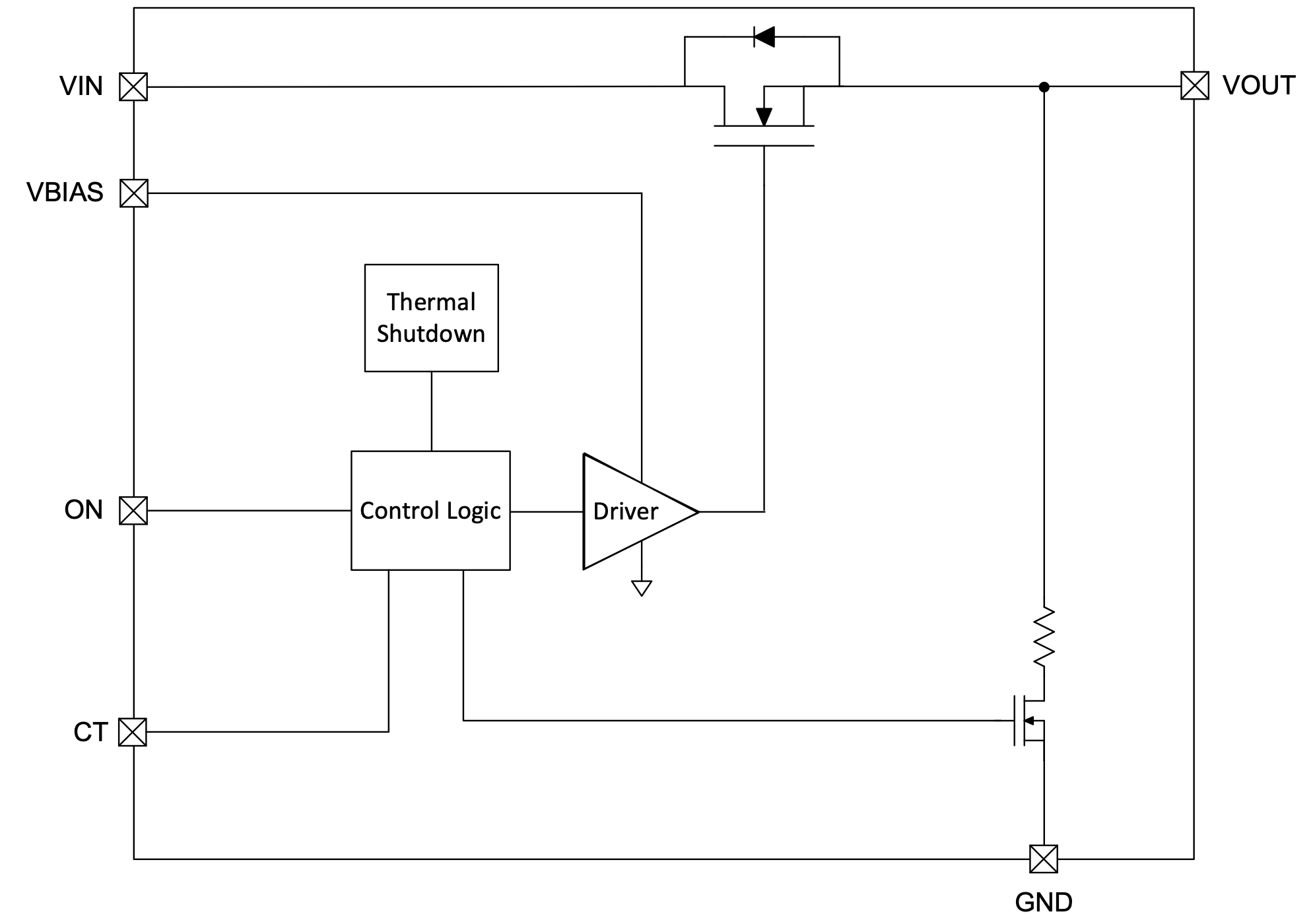
The TPS22998 is a single-channel load switch that provides a configurable rise time to minimize inrush current. The device contains an N-channel MOSFET that can operate over an input voltage range of 0.2 V to 5.5 V and can support a maximum continuous current of 10 A.
The switch is controlled by an on and off input (ON), which is capable of interfacing directly with low voltage control signals (VIH = 0.9 V). The TPS22998 has a fixed quick output discharge when switch is turned off, pulling the output down to ground.
The TPS22998 is available in a 1.5 × 2.0 mm, 0.5 mm pitch, 10-pin WQFN package (RYZ) and is characterized for operation over the free-air temperature range of –40°C to +105°C.
| PART NUMBER | PACKAGE(1) | BODY SIZE (NOM) |
|---|---|---|
TPS22998 | WQFN (10) | 1.5 × 2.0 mm |
 TPS22998 Block Diagram
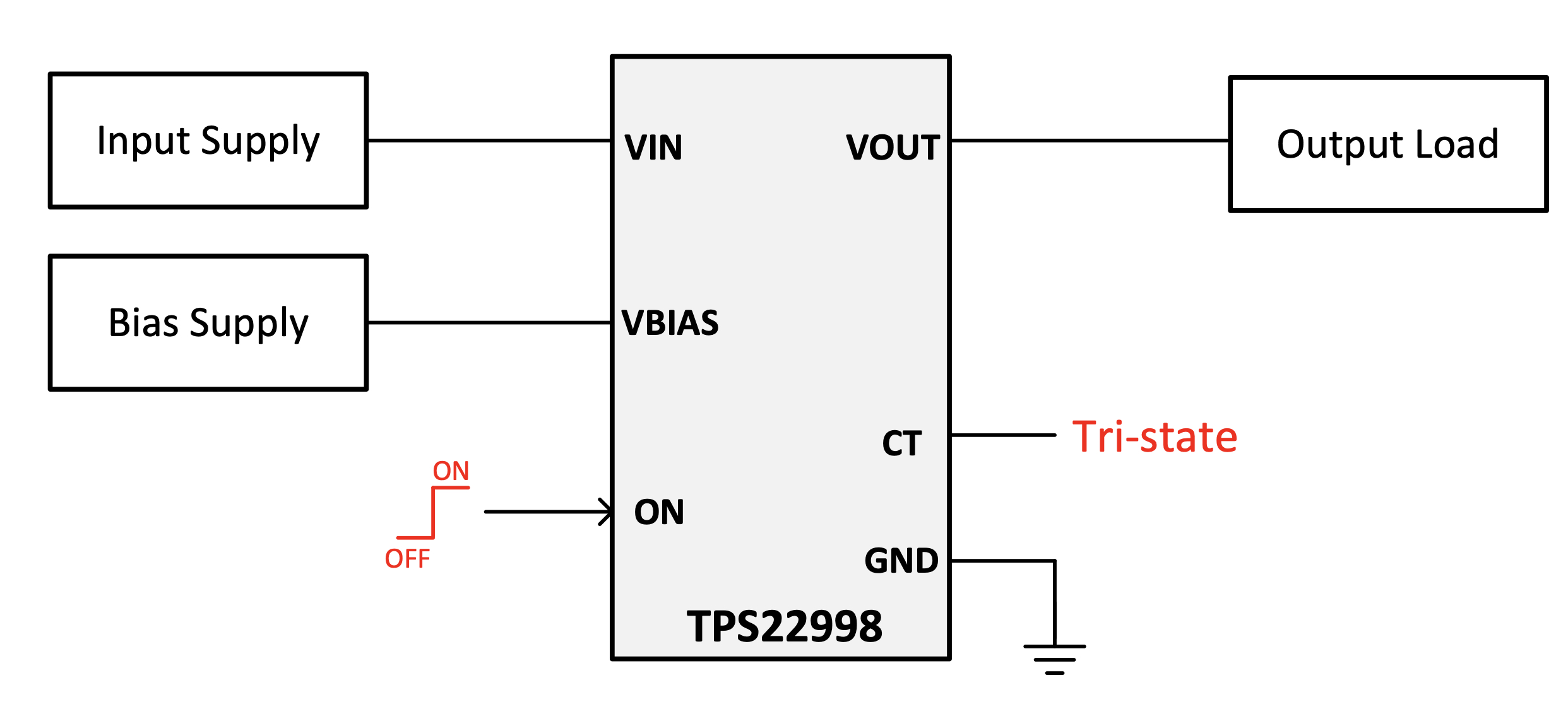
 TPS22998 Typical Application