SLVSDX2A September 2017 – December 2017 TPS23521
PRODUCTION DATA.
- 1 Features
- 2 Applications
- 3 Description
- 4 Revision History
- 5 Pin Configuration and Functions
- 6 Specifications
- 7 Parameter Measurement Information
- 8 Detailed Description
-
9 Application and Implementation
- 9.1 Application Information
- 9.2
Typical Application
- 9.2.1 Design Requirements
- 9.2.2
Detailed Design Procedure
- 9.2.2.1 Selecting RSNS
- 9.2.2.2 Selecting Soft Start Setting: CSS and CSS,VEE
- 9.2.2.3 Selecting VDS Switch Over Threshold
- 9.2.2.4 Timer Selection
- 9.2.2.5 MOSFET Selection and SOA Checks
- 9.2.2.6 EMI Filter Consideration
- 9.2.2.7 Under Voltage and Over Voltage Settings
- 9.2.2.8 Choosing RVCC and CVCC
- 9.2.2.9 Power Good Interface to Downstream DC/DC
- 9.2.3 Application Curves
- 10Power Supply Recommendations
- 11Layout
- 12Device and Documentation Support
- 13Mechanical, Packaging, and Orderable Information
Package Options
Mechanical Data (Package|Pins)
- PW|16
Thermal pad, mechanical data (Package|Pins)
Orderable Information
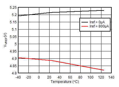
6.7 Typical Characteristics
Unless otherwise noted: –40°C ≤ TJ ≤125°C, 1.1 mA < IVCC< 10 mA, V(UVEN) = 2 V, V(OV) = V(SNS) = V(D) = 0 V, V(SS) = GATEx = Hi-Z , V(TMR) = 0 V, VVref/PG = VPROG = Hi-Z;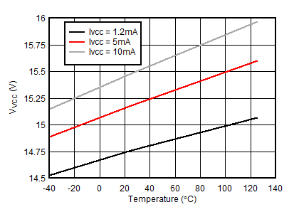
| Ivcc injected into VCC pin |
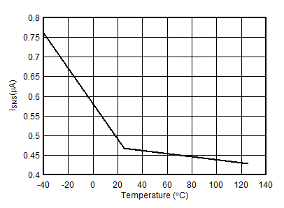
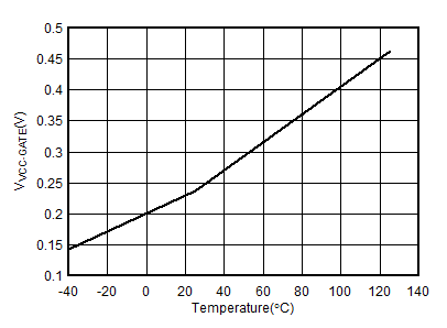
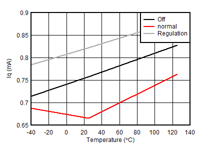
| VVCC = 10 V, Regulation is current limit |
