SLVSDF9A December 2017 – January 2019 TPS23523
PRODUCTION DATA.
- 1 Features
- 2 Applications
- 3 Description
- 4 Revision History
- 5 Pin Configuration and Functions
- 6 Specifications
- 7 Parameter Measurement Information
- 8 Detailed Description
-
9 Application and Implementation
- 9.1 Application Information
- 9.2
Typical Application
- 9.2.1 Design Requirements
- 9.2.2
Detailed Design Procedure
- 9.2.2.1 Selecting RSNS
- 9.2.2.2 Selecting Soft Start Setting: CSS and CSS,VEE
- 9.2.2.3 Selecting VDS Switch Over Threshold
- 9.2.2.4 Timer Selection
- 9.2.2.5 MOSFET Selection and SOA Checks
- 9.2.2.6 Input Cap, Input TVS, and OR-ing FET selection
- 9.2.2.7 EMI Filter Consideration
- 9.2.2.8 Undervoltage and Overvoltage Settings
- 9.2.2.9 Choosing RVCC and CVCC
- 9.2.2.10 Power Good Interface to Downstream DC/DC
- 9.2.3 Application Curves
- 10Power Supply Recommendations
- 11Layout
- 12Device and Documentation Support
- 13Mechanical, Packaging, and Orderable Information
Package Options
Mechanical Data (Package|Pins)
- PW|16
Thermal pad, mechanical data (Package|Pins)
Orderable Information
8.3.1 Current Limit
The TPS23523 utilizes two current limit thresholds:
- ICL1 – also referred to as high current limit threshold, which is used when the VDS of the hot swap FET is low.
- ICL2 – lower current limit threshold, which is used when the VDS of the hot swap FET is high.
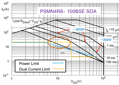
This dual level protection scheme ensures that the part has a higher chance of riding out voltage steps and other transients due to the higher current limit at low VDS, while protecting the MOSFET during start into short and hot-short events, by setting a lower current limit threshold for conditions with high VDS. The transition threshold is programmed with a resistor that is connected from the drain of the hot swap FET to the D pin of the TPS23523. The figure below illustrates an example with a ICL1 set to 25 A and ICL2 set to 3 A. Note that compared to a traditional SOA protection scheme this approach allows better utilization of the SOA in the 10 V < VDS. < 40-V range, which is critical in riding through transients and voltage steps.
Note that in both cases the TPS23523 regulated the gate voltage to enforce the current limit. However, this regulation is not very fast and doesn’t offer the best protection against hot-shorts on the output. To protect in this scenario a fast comparator is used, which quickly pulls down the gate in case of severe over current events (2x bigger than VCL1).
 Figure 8. Dual Current Limit vs FET Power Limit