SLVS933D July 2009 – December 2020 TPS23753A
PRODUCTION DATA
- 1 Features
- 2 Applications
- 3 Description
- 4 Revision History
- 5 Product Information
- 6 Pin Configuration and Functions
- 7 Specifications
-
8 Detailed Description
- 8.1 Overview
- 8.2 Functional Block Diagram
- 8.3 Feature Description
- 8.4
Device Functional Modes
- 8.4.1 Threshold Voltages
- 8.4.2 PoE Start-Up Sequence
- 8.4.3 Detection
- 8.4.4 Hardware Classification
- 8.4.5 Maintain Power Signature (MPS)
- 8.4.6 TPS23753A Operation
- 8.4.7 Special Switching MOSFET Considerations
- 8.4.8 Thermal Considerations
- 8.4.9 FRS and Synchronization
- 8.4.10 Blanking – RBLNK
- 8.4.11 Current Slope Compensation
- 8.4.12 Adapter ORing
- 8.4.13 Protection
- 8.4.14 Frequency Dithering for Conducted Emissions Control
- 9 Application and Implementation
- 10Power Supply Recommendations
- 11Layout
- 12Device and Documentation Support
- 13Mechanical, Packaging, and Orderable Information
Package Options
Mechanical Data (Package|Pins)
- PW|14
Thermal pad, mechanical data (Package|Pins)
Orderable Information
7.7 Typical Characteristics
 Figure 7-1 Detection Bias Current vs Voltage
 Figure 7-3 Converter Start Time vs Temperature
 Figure 7-5 Controller Bias Current vs Temperature
 Figure 7-7 Switching Frequency vs Temperature
 Figure 7-9 Maximum Duty Cycle vs Temperature
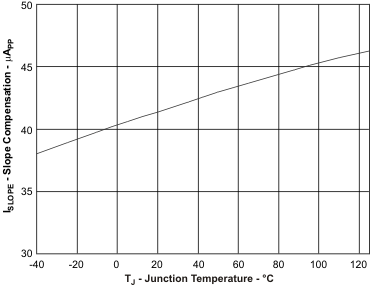
 Figure 7-11 Current Slope Compensation Current vs Temperature
 Figure 7-13 Blanking Period vs RBLNK
 Figure 7-2 PoE Current Limit vs Temperature
 Figure 7-4 Converter Start-Up Source Current vs VVDD1
 Figure 7-6 Controller Bias Current vs Voltage
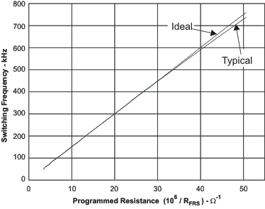
 Figure 7-8 Switching Frequency vs Programmed Resistance
 Figure 7-10 Current Slope Compensation Voltage vs Temperature
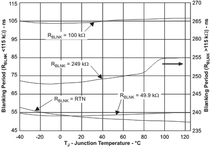
 Figure 7-12 Blanking Period vs Temperature