SLVSDW2B December 2018 – November 2020 TPS23755
PRODUCTION DATA
- 1 Features
- 2 Applications
- 3 Description
- 4 Revision History
- 5 Pin Configuration and Functions
- 6 Specifications
-
7 Detailed Description
- 7.1 Overview
- 7.2 Functional Block Diagram
- 7.3
Feature Description
- 7.3.1 CLS Classification
- 7.3.2 DEN Detection and Enable
- 7.3.3 Internal Pass MOSFET
- 7.3.4
DC-DC Controller Features
- 7.3.4.1 VCC, VB and Advanced PWM Startup
- 7.3.4.2 CS, Current Slope Compensation and Blanking
- 7.3.4.3 COMP, FB, CP and Opto-less Feedback
- 7.3.4.4 FRS Frequency Setting and Synchronization
- 7.3.4.5 Frequency Dithering for Spread Spectrum Applications
- 7.3.4.6 SST and Soft-Start of the Switcher
- 7.3.4.7 AUX_V, AUX_D and Secondary Adapter Or'ing
- 7.3.5 Internal Switching FET - DRAIN, RSNS, SRF and SRR
- 7.3.6 VPD Supply Voltage
- 7.3.7 VDD Supply Voltage
- 7.3.8 GND
- 7.3.9 VSS
- 7.3.10 Exposed Thermal PAD
- 7.4 Device Functional Modes
-
8 Application and Implementation
- 8.1 Application Information
- 8.2
Typical Application
- 8.2.1 Design Requirements
- 8.2.2
Detailed Design Procedure
- 8.2.2.1 Input Bridges and Schottky Diodes
- 8.2.2.2 Protection, D1
- 8.2.2.3 Capacitor, C1
- 8.2.2.4 Detection Resistor, RDEN
- 8.2.2.5 Classification Resistor, RCLS
- 8.2.2.6 Bulk Capacitance, CBULK
- 8.2.2.7 Output Voltage Feedback Divider, RAUX, R1,R2
- 8.2.2.8 Setting Frequency, RFRS
- 8.2.2.9 Frequency Dithering, RDTR and CDTR
- 8.2.2.10 Bias Voltage, CVB and DVB
- 8.2.2.11 Transformer design, T1
- 8.2.2.12 Current Sense Resistor, RCS
- 8.2.2.13 Current Slope Compensation, RS
- 8.2.2.14 Bias Supply Requirements, CCC, DCC
- 8.2.2.15 Switching Transformer Considerations, RVCC and CCC2
- 8.2.2.16 Primary FET Clamping, RCL, CCL, and DCL
- 8.2.2.17 Converter Output Capacitance, COUT
- 8.2.2.18 Secondary Output Diode Rectifier, DOUT
- 8.2.2.19 Slew rate control, RSRF and RSRR
- 8.2.2.20 Shutdown at Low Temperatures, DVDD and CVDD
- 8.2.3 Application Curves
- 9 Power Supply Recommendations
- 10Layout
- 11Device and Documentation Support
- 12Mechanical, Packaging, and Orderable Information
Package Options
Mechanical Data (Package|Pins)
- RJJ|23
Thermal pad, mechanical data (Package|Pins)
Orderable Information
6.7 Typical Characteristics
 Figure 6-1 Detection Bias Current vs Voltage
 Figure 6-3 PoE
Inrush Current Limit vs Temperature
 Figure 6-5 VPD
and VDD Supply Current vs Voltage
 Figure 6-7 Converter Soft-Start Time vs Temperature
 Figure 6-9 Switching Frequency vs Temperature
 Figure 6-11 Frequency Dithering Charging Current
 Figure 6-13 Frequency Dithering Peak-to-Peak Amplitude
 Figure 6-15 Current Slope Compensation Current vs Temperature
 Figure 6-17 Converter PWM Comparator Delay vs Temperature
 Figure 6-19 Error
Amplifier Source Current
 Figure 6-21 Error
Amplifier Gain vs Frequency
 Figure 6-23 Switching FET Resistance vs Temperature
 Figure 6-2 PoE
Current Limit vs Temperature
 Figure 6-4 Pass
FET Resistance vs Temperature
 Figure 6-6 Converter Startup Time vs Temperature
 Figure 6-8 Controller Bias Current vs Voltage
 Figure 6-10 Switching Frequency vs Programmed Resistance
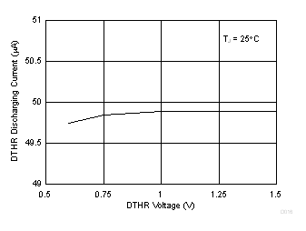
 Figure 6-12 Frequency Dithering Discharging Current
 Figure 6-14 Feedback Regulation Voltage vs Temperature
 Figure 6-16 Blanking Period vs Temperature
 Figure 6-18 Converter Current Limit Delay vs Temperature
 Figure 6-20 Error
Amplifier Sink Current
 Figure 6-22 Error
Amplifier Phase vs Frequency