SLVS646B September 2006 – November 2018 TPS2376-H
PRODUCTION DATA.
- 1 Features
- 2 Applications
- 3 Description
- 4 Revision History
- 5 Device Comparison Table
- 6 Pin Configuration and Functions
- 7 Specifications
- 8 Detailed Description
- 9 Application and Implementation
- 10Power Supply Recommendations
- 11Layout
- 12Device and Documentation Support
- 13Mechanical, Packaging, and Orderable Information
Package Options
Mechanical Data (Package|Pins)
- DDA|8
Thermal pad, mechanical data (Package|Pins)
- DDA|8
Orderable Information
10.3 Auxiliary Power Source ORing
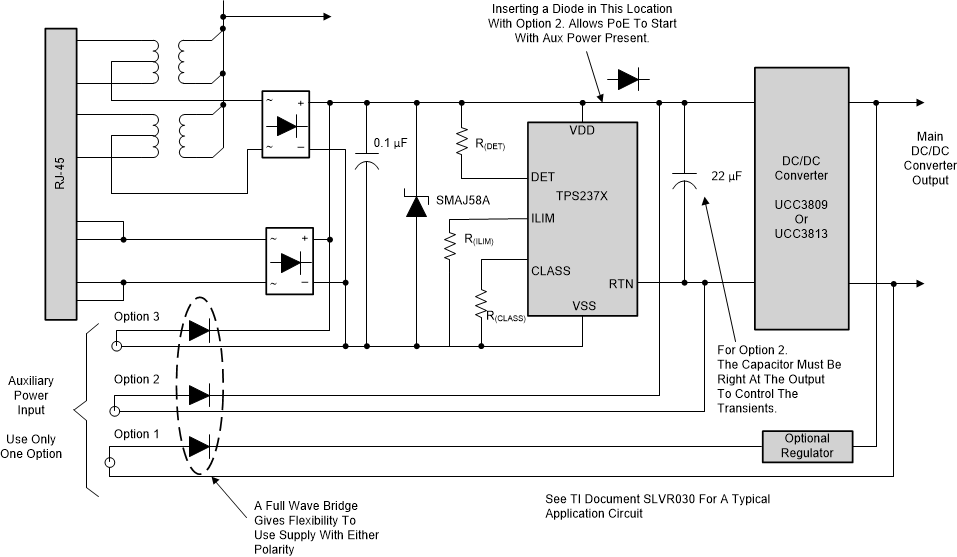
Many PoE-capable devices are designed to operate from either a wall adapter or PoE power. A local power solution adds cost and complexity, but allows a product to be used regardless of PoE availability. Attempting to create solutions where the two power sources coexist in a specific controlled manner results in additional complexity, and is not generally recommended. Figure 14 demonstrates three methods of diode ORing external power into a PD. Option 1 inserts power on the output side of the PoE power conversion. Option 2 inserts power on the TPS2376-H output. Option 3 applies power to the TPS2376-H input. Each of these options has advantages and disadvantages. The wall adapter must meet a minimum 1500-Vac dielectric withstand test voltage to the ac input power and to ground for options 2 and 3.
 Figure 14. Auxiliary Power ORing
 Option 1 consists of ORing power to the output of the PoE dc/dc converter. This option is preferred in cases where PoE is added to an existing design that uses a low-voltage wall adapter. The relatively large PD capacitance reduces the potential for harmful transients when the adapter is plugged in. The wall adapter output may be grounded if the PD incorporates an isolated converter. This solution requires two separate regulators, but low-voltage adapters are readily available. The PoE power can be given priority by setting its output voltage above the adapter's.
Option 2 has the benefits that the adapter voltage may be lower than the TPS2376-H UVLO, and that the bulk capacitor shown controls voltage transients caused by plugging an adapter in. The capacitor size and location are chosen to control the amount of ringing that can occur on this node, which can be affected by additional filtering components specific to a dc/dc converter design. The optional diode blocks the adapter voltage from reverse biasing the input, and allows a PoE source to supply power provided that the PSE output voltage is greater than the adapter voltage. The penalty of the diode is an additional power loss when running from PSE power. The PSE may not be able to detect and start powering without the diode. This means that the adapter may continue to power the PD until removed. Auxiliary voltage sources can be selected to be above or below the PoE operational voltage range. If automatic PoE precedence is desired when using the low-voltage auxiliary source option, make sure that the TPS2376-H inrush program limit is set higher than the maximum converter input current at its lowest operating voltage. It is difficult to use PG with the low-voltage auxiliary source because the converter must operate during a condition when the TPS2376-H would normally disable it. Circuits may be designed to force operation from one source or the other depending on the desired operation and the auxiliary source voltage chosen. However, they are not recommended because they increase complexity and thus cost.
Option 3 inserts the power before the TPS2376-H. The adapter output voltage must meet the TPS2376-H UVLO turn-on requirement and limit the maximum voltage to 57 V. This option provides a valid power-good signal and simplifies power priority issues. Option 3 is the most likely to create transient voltage problems when a powered adapter is plugged in. This causes the cabling inductance and PD input capacitance to ring to a high voltage that must be clamped by the TVS. If the adapter applies voltage to the PD before the PSE, it prevents the PSE from detecting the PD. If the PSE is already powering the PD when the adapter is plugged in, priority is given to the higher supply voltage.