SLVSB99C March 2012 – July 2015 TPS2378
PRODUCTION DATA.
- 1 Features
- 2 Applications
- 3 Description
- 4 Revision History
- 5 Pin Configuration and Functions
- 6 Specifications
-
7 Detailed Description
- 7.1 Overview
- 7.2 Functional Block Diagram
- 7.3 Feature Description
- 7.4
Device Functional Modes
- 7.4.1 PoE Overview
- 7.4.2 Threshold Voltages
- 7.4.3 PoE Start-up Sequence
- 7.4.4 Detection
- 7.4.5 Hardware Classification
- 7.4.6 Inrush and Start-up
- 7.4.7 Maintain Power Signature
- 7.4.8 Start-up and Converter Operation
- 7.4.9 PD Hotswap Operation
- 7.4.10 Start-up and Power Management, CDB and T2P
- 7.4.11 Adapter ORing
- 7.4.12 Using DEN to Disable PoE
- 7.4.13 ORing Challenges
- 8 Application and Implementation
- 9 Power Supply Recommendations
- 10Layout
- 11Device and Documentation Support
- 12Mechanical, Packaging, and Orderable Information
Package Options
Mechanical Data (Package|Pins)
- DDA|8
Thermal pad, mechanical data (Package|Pins)
- DDA|8
Orderable Information
10 Layout
10.1 Layout Guidelines
The layout of the PoE front end should follow power and EMI/ESD best practice guidelines. A basic set of recommendations include:
- Parts placement must be driven by power flow in a point-to-point manner; RJ-45, Ethernet transformer, diode bridges, TVS and 0.1-μF capacitor, and TPS2378.
- All leads should be as short as possible with wide power traces and paired signal and return.
- There should not be any crossovers of signals from one part of the flow to another.
- Spacing consistent with safety standards like IEC60950 must be observed between the 48-V input voltage rails and between the input and an isolated converter output.
- The TPS2378 should be located over split, local ground planes referenced to VSS for the PoE input and to RTN for the switched output.
- Large copper fills and traces should be used on SMT power-dissipating devices, and wide traces or overlay copper fills should be used in the power path.
10.2 Layout Example
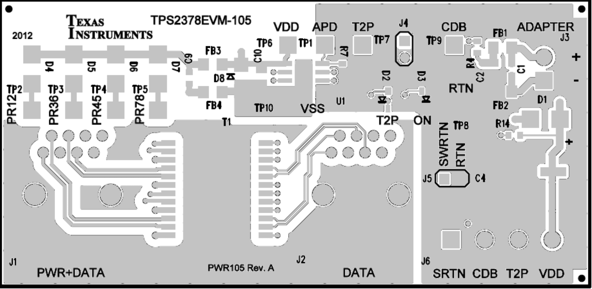
Figure 27 and Figure 28 show the top and bottom layer and assemblies of the TPS2378EVM-105 as a reference for optimum parts placement. A detailed PCB layout can be found in the user’s guide of the TPS2378EVM-105 (SLVU682).
 Figure 27. Top Side
 Figure 28. Bottom Side
10.3 EMI Containment
- Use compact loops for dv/dt and di/dt circuit paths (power loops and gate drives).
- Use minimal, yet thermally adequate, copper areas for heat sinking of components tied to switching nodes (minimize exposed radiating surface).
- Use copper ground planes (possible stitching) and top layer copper floods (surround circuitry with ground floods).
- Use 4 layer PCB if economically feasible (for better grounding).
- Minimize the amount of copper area associated with input traces (to minimize radiated pickup).
- Use Bob Smith terminations, Bob Smith EFT capacitor, and Bob Smith plane.
- Use Bob Smith plane as ground shield on input side of PCB (creating a phantom or literal earth ground).
- Use of ferrite beads on input (allow for possible use of beads or 0 ohm resistors).
- Maintain physical separation between input-related circuitry and power circuitry (use ferrite beads as boundary line).
- Possible use of common-mode inductors.
- Possible use of integrated RJ-45 jacks (shielded with internal transformer and Bob Smith terminations).
- End-product enclosure considerations (shielding).
10.4 Thermal Considerations and OTSD
Sources of nearby local PCB heating should be considered during the thermal design. Typical calculations assume that the TPS2378 is the only heat source contributing to the PCB temperature rise. It is possible for a normally operating TPS2378 device to experience an OTSD event if it is excessively heated by a nearby device.
10.5 ESD
ESD requirements for a unit that incorporates the TPS2378 have a much broader scope and operational implications than are used in TI’s testing. Unit-level requirements should not be confused with reference design testing that only validates the ruggedness of the TPS2378.