SLUS634F November 2004 – January 2022 TPS2384
PRODUCTION DATA
- 1 Features
- 2 Applications
- 3 Description
- 4 Revision History
- 5 Pin Configuration and Functions
- 6 Specifications
- 7 Parameter Measurement Information
-
8 Detailed Description
- 8.1 Overview
- 8.2 Functional Block Diagrams
- 8.3 Feature Description
- 8.4
Device Functional Modes
- 8.4.1 Auto Mode
- 8.4.2 Auto Mode Functional Description
- 8.4.3 AM Faults and INTB Output
- 8.4.4 Over and Undervoltage Fault
- 8.4.5 Over Current or Current Limit Faults
- 8.4.6 Undercurrent Fault (DC Modulated Disconnect)
- 8.4.7 Power Management Mode (PMM)
- 8.4.8 PMM Discovery 1
- 8.4.9 PMM Discovery 2
- 8.4.10 PMM Classification
- 8.4.11 PMM Legacy
- 8.4.12 PMM Rup Pwr
- 8.4.13 PMM RDWN
- 8.5 Programming
- 8.6
Register Maps
- 8.6.1 Register/Port Addressing Map
- 8.6.2 Common Read, Register Select
- 8.6.3 Common Write, Register Select = 1111 (Test Register)
- 8.6.4 Common Control Write, Register Select = 0001
- 8.6.5 Port Control Write 1, Register Select = 0010 (One Per Port)
- 8.6.6 Port Control Write 2, Register Select = 0011 (One Per Port)
- 8.6.7 Port Status Read 1, Register Select = 0100 (One Per Port)
- 8.6.8 Port Status Read 2, Register Select = 0101 (One Per Port)
- 8.6.9
A/D Results Registers (Discovery Current, Voltage, Current and Temperature)
- 8.6.9.1 Discovery Current — Lower Bits, Register Select = 0110 (One Per Port)
- 8.6.9.2 Discovery Current — Upper Bits, Register Select = 0111 (One Per Port)
- 8.6.9.3 Voltage — Lower Bits, Register Select = 1000 (One Per Port)
- 8.6.9.4 Voltage — Upper Bits, Register Select = 1001 (One Per Port)
- 8.6.9.5 Current — Lower Bits, Register Select = 1010 (One Per Port)
- 8.6.9.6 Current — Upper Bits, Register Select = 1011 (One Per Port)
- 8.6.9.7 Temperature — Lower Bits, Register Select = 1100 (One Per Port)
- 8.6.9.8 Temperature — Upper Bits, Register Select = 1101 (One Per Port)
- 9 Application and Implementation
- 10Power Supply Recommendations
- 11Layout
- 12Device and Documentation Support
- 13Mechanical, Packaging, and Orderable Information
Package Options
Mechanical Data (Package|Pins)
Thermal pad, mechanical data (Package|Pins)
Orderable Information
8.4.6 Undercurrent Fault (DC Modulated Disconnect)
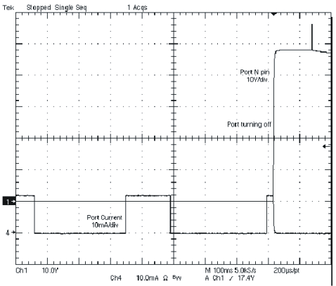
Undercurrent fault (dc modulated disconnect) is a condition when the load current that is being measured drops below 7.5 mA and turns on the disconnect timer. If the disconnect timer reaches its time out limit that is set between 300 ms to 400 ms, the corresponding port is turned off and the load disconnect fault code is generated in the Port Status 1 register. If the undercurrent condition goes away prior to the disconnect timer reaching its limit the timer is reset and the port remains powered.
Figure 8-10 shows DC Disconnect event. In this setup, the load current was set right above the 7.5-mA threshold. The duty cycle of the load was then adjusted until the off period exceeded the disconnect time out, causing turn-off of the port. The time-out period was > 300 ms.
 Figure 8-10 Port Undercurrent
Response in DC Disconnect