SLUSD53G March 2018 – August 2020 TPS23880
PRODUCTION DATA
- 1 Features
- 2 Applications
- 3 Description
- 4 Revision History
- 5 Device Comparison Table
- 6 Pin Configuration and Functions
- 7 Specifications
- 8 Parameter Measurement Information
-
9 Detailed Description
- 9.1 Overview
- 9.2 Functional Block Diagram
- 9.3 Feature Description
- 9.4 Device Functional Modes
- 9.5 I2C Programming
- 9.6
Register Maps
- 9.6.1 Complete Register Set
- 9.6.2
Detailed Register Descriptions
- 9.6.2.1 INTERRUPT Register
- 9.6.2.2 INTERRUPT MASK Register
- 9.6.2.3 POWER EVENT Register
- 9.6.2.4 DETECTION EVENT Register
- 9.6.2.5 FAULT EVENT Register
- 9.6.2.6 START/ILIM EVENT Register
- 9.6.2.7 SUPPLY and FAULT EVENT Register
- 9.6.2.8 CHANNEL 1 DISCOVERY Register
- 9.6.2.9 CHANNEL 2 DISCOVERY Register
- 9.6.2.10 CHANNEL 3 DISCOVERY Register
- 9.6.2.11 CHANNEL 4 DISCOVERY Register
- 9.6.2.12 POWER STATUS Register
- 9.6.2.13 PIN STATUS Register
- 9.6.2.14 OPERATING MODE Register
- 9.6.2.15 DISCONNECT ENABLE Register
- 9.6.2.16 DETECT/CLASS ENABLE Register
- 9.6.2.17 Power Priority / 2Pair PCUT Disable Register Name
- 9.6.2.18 TIMING CONFIGURATION Register
- 9.6.2.19 GENERAL MASK Register
- 9.6.2.20 DETECT/CLASS RESTART Register
- 9.6.2.21 POWER ENABLE Register
- 9.6.2.22 RESET Register
- 9.6.2.23 ID Register
- 9.6.2.24 Connection Check and Auto Class Status Register
- 9.6.2.25 2-Pair Police Ch-1 Configuration Register
- 9.6.2.26 2-Pair Police Ch-2 Configuration Register
- 9.6.2.27 2-Pair Police Ch-3 Configuration Register
- 9.6.2.28 2-Pair Police Ch-4 Configuration Register
- 9.6.2.29 Power-on Fault Register
- 9.6.2.30 PORT RE-MAPPING Register
- 9.6.2.31 Channels 1 and 2 Multi Bit Priority Register
- 9.6.2.32 Channels 3 and 4 Multi Bit Priority Register
- 9.6.2.33 4-Pair Wired and Port Power Allocation Register
- 9.6.2.34 4-Pair Police Ch-1 and 2 Configuration Register
- 9.6.2.35 4-Pair Police Ch-3 and 4 Configuration Register
- 9.6.2.36 TEMPERATURE Register
- 9.6.2.37 4-Pair Fault Configuration Register
- 9.6.2.38 INPUT VOLTAGE Register
- 9.6.2.39 CHANNEL 1 CURRENT Register
- 9.6.2.40 CHANNEL 2 CURRENT Register
- 9.6.2.41 CHANNEL 3 CURRENT Register
- 9.6.2.42 CHANNEL 4 CURRENT Register
- 9.6.2.43 CHANNEL 1 VOLTAGE Register
- 9.6.2.44 CHANNEL 2 VOLTAGE Register
- 9.6.2.45 CHANNEL 3 VOLTAGE Register
- 9.6.2.46 CHANNEL 4 VOLTAGE Register
- 9.6.2.47 2x FOLDBACK SELECTION Register
- 95
- 9.6.2.48 FIRMWARE REVISION Register
- 9.6.2.49 I2C WATCHDOG Register
- 9.6.2.50 DEVICE ID Register
- 9.6.2.51 CHANNEL 1 DETECT RESISTANCE Register
- 9.6.2.52 CHANNEL 2 DETECT RESISTANCE Register
- 9.6.2.53 CHANNEL 3 DETECT RESISTANCE Register
- 9.6.2.54 CHANNEL 4 DETECT RESISTANCE Register
- 9.6.2.55 CHANNEL 1 ASSIGNED CLASS Register
- 9.6.2.56 CHANNEL 2 ASSIGNED CLASS Register
- 9.6.2.57 CHANNEL 3 ASSIGNED CLASS Register
- 9.6.2.58 CHANNEL 4 ASSIGNED CLASS Register
- 9.6.2.59 AUTO CLASS CONTROL Register
- 9.6.2.60 CHANNEL 1 AUTO CLASS POWER Register
- 9.6.2.61 CHANNEL 2 AUTO CLASS POWER Register
- 9.6.2.62 CHANNEL 3 AUTO CLASS POWER Register
- 9.6.2.63 CHANNEL 4 AUTO CLASS POWER Register
- 9.6.2.64 ALTERNATIVE FOLDBACK Register
- 9.6.2.65 SRAM CONTROL Register
- 10Application and Implementation
- 11Power Supply Recommendations
- 12Layout
- 13Device and Documentation Support
- 14Mechanical, Packaging, and Orderable Information
Package Options
Mechanical Data (Package|Pins)
- RTQ|56
Thermal pad, mechanical data (Package|Pins)
- RTQ|56
Orderable Information
3 Description
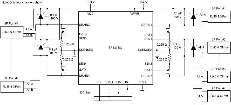
The TPS23880 is an 8-channel power sourcing equipment (PSE) controller engineered to insert power onto Ethernet cables in accordance with the IEEE 802.3bt standard. The eight individual power channels can be configured in any combination of 2-Pair (1-channel) or 4-Pair (2-channels) PoE Ports. The PSE controller can detect powered devices (PDs) that have a valid signature, complete mutual identification, and apply power.
Programmable SRAM enables in-field firmware upgradability over I2C to ensure IEEE compliance and interoperability with the latest PoE enabled devices. Dedicated per port ADCs provide continuous port current monitoring and the ability to perform parallel classification measurements for faster port turn on times. A ±3% accurate programmable port power limit provides the ability to expand the maximum power sourced above 90 W without exceeding 100 W while also making system level power management control more easy to implement and reliable. The Fast Shutdown (OSS) input provides up to eight levels of per port shutdown priority for applications requiring immediate disabling of multiple ports. The 255-mΩ current sense resistor and external FET architecture allow designs to balance size, efficiency, thermal and solution cost requirements.
Port remapping and pin-to-pin compatibility with the TPS2388, TPS23881, and TPS23882 devices eases migration from previous generation PSE designs and enables interchangeable 2-layer PCB designs to accommodate different system PoE power configurations.
| PART NUMBER | PACKAGE | BODY SIZE (NOM) |
|---|---|---|
| TPS23880 | VQFN (56) | 8.00 mm × 8.00 mm |
 Simplified Schematic