SLVSF02E march 2019 – may 2023 TPS23881
PRODUCTION DATA
- 1
- 1 Features
- 2 Applications
- 3 Description
- 4 Revision History
- 5 Device Comparison Table
- 6 Pin Configuration and Functions
- 7 Specifications
- 8 Parameter Measurement Information
-
9 Detailed Description
- 9.1 Overview
- 9.2 Functional Block Diagram
- 9.3 Feature Description
- 9.4 Device Functional Modes
- 9.5 I2C Programming
- 9.6
Register Maps
- 9.6.1 Complete Register Set
- 9.6.2
Detailed Register Descriptions
- 9.6.2.1 INTERRUPT Register
- 9.6.2.2 INTERRUPT MASK Register
- 9.6.2.3 POWER EVENT Register
- 9.6.2.4 DETECTION EVENT Register
- 9.6.2.5 FAULT EVENT Register
- 9.6.2.6 START/ILIM EVENT Register
- 9.6.2.7 SUPPLY and FAULT EVENT Register
- 9.6.2.8 CHANNEL 1 DISCOVERY Register
- 9.6.2.9 CHANNEL 2 DISCOVERY Register
- 9.6.2.10 CHANNEL 3 DISCOVERY Register
- 9.6.2.11 CHANNEL 4 DISCOVERY Register
- 9.6.2.12 POWER STATUS Register
- 9.6.2.13 PIN STATUS Register
- 9.6.2.14 OPERATING MODE Register
- 9.6.2.15 DISCONNECT ENABLE Register
- 9.6.2.16 DETECT/CLASS ENABLE Register
- 9.6.2.17 Power Priority / 2Pair PCUT Disable Register Name
- 9.6.2.18 TIMING CONFIGURATION Register
- 9.6.2.19 GENERAL MASK Register
- 9.6.2.20 DETECT/CLASS RESTART Register
- 9.6.2.21 POWER ENABLE Register
- 9.6.2.22 RESET Register
- 9.6.2.23 ID Register
- 9.6.2.24 Connection Check and Auto Class Status Register
- 9.6.2.25 2-Pair Police Ch-1 Configuration Register
- 9.6.2.26 2-Pair Police Ch-2 Configuration Register
- 9.6.2.27 2-Pair Police Ch-3 Configuration Register
- 9.6.2.28 2-Pair Police Ch-4 Configuration Register
- 9.6.2.29 Capacitance (Legacy PD) Detection
- 9.6.2.30 Power-on Fault Register
- 9.6.2.31 PORT RE-MAPPING Register
- 9.6.2.32 Channels 1 and 2 Multi Bit Priority Register
- 9.6.2.33 Channels 3 and 4 Multi Bit Priority Register
- 9.6.2.34 4-Pair Wired and Port Power Allocation Register
- 9.6.2.35 4-Pair Police Ch-1 and 2 Configuration Register
- 9.6.2.36 4-Pair Police Ch-3 and 4 Configuration Register
- 9.6.2.37 TEMPERATURE Register
- 9.6.2.38 4-Pair Fault Configuration Register
- 9.6.2.39 INPUT VOLTAGE Register
- 9.6.2.40 CHANNEL 1 CURRENT Register
- 9.6.2.41 CHANNEL 2 CURRENT Register
- 9.6.2.42 CHANNEL 3 CURRENT Register
- 9.6.2.43 CHANNEL 4 CURRENT Register
- 9.6.2.44 CHANNEL 1 VOLTAGE Register
- 9.6.2.45 CHANNEL 2 VOLTAGE Register
- 9.6.2.46 CHANNEL 3 VOLTAGE Register
- 9.6.2.47 CHANNEL 4 VOLTAGE Register
- 9.6.2.48 2x FOLDBACK SELECTION Register
- 9.6.2.49 FIRMWARE REVISION Register
- 9.6.2.50 I2C WATCHDOG Register
- 9.6.2.51 DEVICE ID Register
- 9.6.2.52 CHANNEL 1 DETECT RESISTANCE Register
- 9.6.2.53 CHANNEL 2 DETECT RESISTANCE Register
- 9.6.2.54 CHANNEL 3 DETECT RESISTANCE Register
- 9.6.2.55 CHANNEL 4 DETECT RESISTANCE Register
- 9.6.2.56 CHANNEL 1 DETECT CAPACITANCE Register
- 9.6.2.57 CHANNEL 2 DETECT CAPACITANCE Register
- 9.6.2.58 CHANNEL 3 DETECT CAPACITANCE Register
- 9.6.2.59 CHANNEL 4 DETECT CAPACITANCE Register
- 9.6.2.60 CHANNEL 1 ASSIGNED CLASS Register
- 9.6.2.61 CHANNEL 2 ASSIGNED CLASS Register
- 9.6.2.62 CHANNEL 3 ASSIGNED CLASS Register
- 9.6.2.63 CHANNEL 4 ASSIGNED CLASS Register
- 9.6.2.64 AUTO CLASS CONTROL Register
- 9.6.2.65 CHANNEL 1 AUTO CLASS POWER Register
- 9.6.2.66 CHANNEL 2 AUTO CLASS POWER Register
- 9.6.2.67 CHANNEL 3 AUTO CLASS POWER Register
- 9.6.2.68 CHANNEL 4 AUTO CLASS POWER Register
- 9.6.2.69 ALTERNATIVE FOLDBACK Register
- 9.6.2.70 SRAM CONTROL Register
- 10Application and Implementation
- 11Power Supply Recommendations
- 12Layout
- 13Device and Documentation Support
- 14Mechanical, Packaging, and Orderable Information
Package Options
Mechanical Data (Package|Pins)
- RTQ|56
Thermal pad, mechanical data (Package|Pins)
- RTQ|56
Orderable Information
3 Description
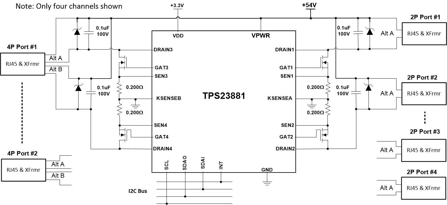
The TPS23881 is an 8-channel power sourcing equipment (PSE) controller engineered to insert power onto Ethernet cables in accordance with the IEEE 802.3bt standard. The eight individual power channels can be configured in any combination of 2-Pair (1-channel) or 4-Pair (2-channels) PoE Ports. The PSE controller can detect powered devices (PDs) that have a valid signature, complete mutual identification, and apply power.
The TPS23881 improves on the TPS23880 with reduced current sense resistors, more accurate programmable power limiting, capacitance measurement and the ability to operate from ROM (see Device Comparison Table). The TPS23881 is also compatible with TI's FirmPSE system firmware, which provides a fully configurable solution for controlling multiple TPS23881 devices in systems offering up to 48-ports of 4-pair PoE power.
Programmable SRAM enables in-field firmware upgradability over I2C to ensure IEEE compliance and interoperability with the latest PoE enabled devices. Dedicated per port ADCs provide continuous port current monitoring and the ability to perform parallel classification measurements for faster port turn on times. A ±2.5% accurate programmable port power limit provides the ability to expand the maximum power sourced from 90 W to upwards of 125 W. The 200-mΩ current sense resistor and external FET architecture allow designs to balance size, efficiency, thermal and solution cost requirements.
| PART NUMBER | PACKAGE | BODY SIZE (NOM) |
|---|---|---|
| TPS23881 | VQFN (56) | 8.00 mm × 8.00 mm |
 Simplified Schematic