SLVSAL2G January 2011 – November 2015 TPS24710 , TPS24711 , TPS24712 , TPS24713
PRODUCTION DATA.
- 1 Features
- 2 Applications
- 3 Description
- 4 Revision History
- 5 Device Comparison Table
- 6 Pin Configuration and Functions
- 7 Specifications
- 8 Detailed Description
-
9 Application and Implementation
- 9.1 Application Information
- 9.2
Typical Application
- 9.2.1 Design Requirements
- 9.2.2
Detailed Design Procedure
- 9.2.2.1
Power-Limited Start-Up
- 9.2.2.1.1 STEP 1. Choose RSENSE
- 9.2.2.1.2 STEP 2. Choose MOSFET M1
- 9.2.2.1.3 STEP 3. Choose Power-Limit Value, PLIM, and RPROG
- 9.2.2.1.4 STEP 4. Choose Output Voltage Rising Time, tON, CT
- 9.2.2.1.5 STEP 5. Calculate the Retry-Mode Duty Ratio
- 9.2.2.1.6 STEP 6. Select R1 and R2 for UV
- 9.2.2.1.7 STEP 7. Choose RGATE, R4, R5 and C1
- 9.2.2.2 Additional Design Considerations
- 9.2.2.1
Power-Limited Start-Up
- 9.2.3 Application Curve
- 10Power Supply Recommendations
- 11Layout
- 12Device and Documentation Support
- 13Mechanical, Packaging, and Orderable Information
Package Options
Mechanical Data (Package|Pins)
- DGS|10
Thermal pad, mechanical data (Package|Pins)
Orderable Information
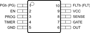
6 Pin Configuration and Functions
DGS Package
(10 Pins)
Top View

Pin Functions
| PINS | I/O | DESCRIPTION | ||
|---|---|---|---|---|
| NAME | TPS24710/11 | TPS24712/13 | ||
| EN | 2 | 2 | I | Active-high enable input. Logic input. Connects to resistor divider. |
| FLT | – | 10 | O | Active-high, open-drain output indicates overload fault timer has turned MOSFET off. |
| FLTb | 10 | – | Active-low, open-drain output indicates overload fault timer has turned MOSFET off. | |
| GATE | 7 | 7 | O | Gate driver output for external MOSFET |
| GND | 5 | 5 | – | Ground |
| OUT | 6 | 6 | I | Output voltage sensor for monitoring MOSFET power. |
| PG | – | 1 | O | Active-high, open-drain power good indicator. Status is determined by the voltage across the MOSFET. |
| PGb | 1 | – | Active-low, open-drain power good indicator. Status is determined by the voltage across the MOSFET. | |
| PROG | 3 | 3 | I | Power-limiting programming pin. A resistor from this pin to GND sets the maximum power dissipation for the FET. |
| SENSE | 8 | 8 | I | Current sensing input for resistor shunt from VCC to SENSE. |
| TIMER | 4 | 4 | I/O | A capacitor connected from this pin to GND provides a fault timing function. |
| VCC | 9 | 9 | I | Input-voltage sense and power supply |