SLVSAL1E March 2011 – April 2016 TPS24720
PRODUCTION DATA.
- 1 Features
- 2 Applications
- 3 Description
- 4 Revision History
- 5 Pin Configuration and Functions
- 6 Specifications
-
7 Detailed Description
- 7.1 Overview
- 7.2 Functional Block Diagram
- 7.3 Feature Description
- 7.4
Device Functional Modes
- 7.4.1 Board Plug-In
- 7.4.2 Inrush Operation
- 7.4.3 Action of the Constant-Power Engine
- 7.4.4 Circuit Breaker and Fast Trip
- 7.4.5 Automatic Restart
- 7.4.6 PGb, FLTb, and Timer Operations
- 7.4.7 Overtemperature Shutdown
- 7.4.8 Start-Up of Hot-Swap Circuit by VCC or EN
- 7.4.9 Minimization of Power Dissipation at STANDY by ENSD
- 7.4.10 Fault Detection of MOSFET Short With FFLTb
-
8 Application and Implementation
- 8.1 Application Information
- 8.2
Typical Application
- 8.2.1 Design Requirements
- 8.2.2
Detailed Design Procedure
- 8.2.2.1
Power-Limited Start-Up
- 8.2.2.1.1 STEP 1. Choose RSENSE, RSET, and RIMON
- 8.2.2.1.2 STEP 2. Choose MOSFET M1
- 8.2.2.1.3 STEP 3. Choose Power-Limit Value, PLIM, and RPROG
- 8.2.2.1.4 STEP 4. Choose Output Voltage Rising Time, tON, and Timing Capacitor CT
- 8.2.2.1.5 STEP 5. Calculate the Retry-Mode Duty Ratio
- 8.2.2.1.6 STEP 6. Select R1, R2, and R3 for UV and OV
- 8.2.2.1.7 STEP 7. Choose RGATE, R4, R5, R6, and C1
- 8.2.2.2 Additional Design Considerations
- 8.2.2.1
Power-Limited Start-Up
- 8.2.3 Application Curve
- 9 Power Supply Recommendations
- 10Layout
- 11Device and Documentation Support
- 12Mechanical, Packaging, and Orderable Information
Package Options
Mechanical Data (Package|Pins)
- RGT|16
Thermal pad, mechanical data (Package|Pins)
- RGT|16
Orderable Information
7 Detailed Description
7.1 Overview
7.3 Feature Description
7.3.1 Detailed Pin Descriptions
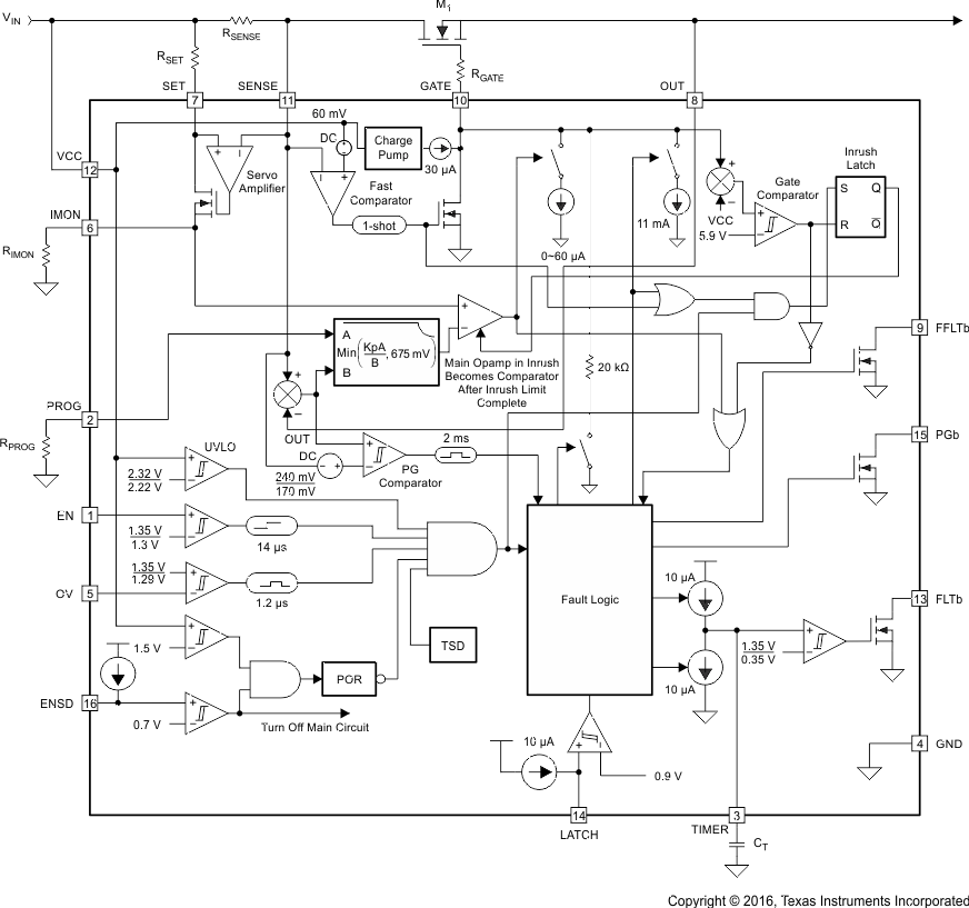
The following description relies on the typical application diagram shown on the front page of this data sheet, as well as the functional block diagram in Figure 28.
7.3.1.1 EN
Applying a voltage of 1.35 V or more to this pin enables the gate driver. The addition of an external resistor divider allows the EN pin to serve as an undervoltage monitor. Cycling EN low and then back high resets the TPS24720 that has latched off due to a fault condition. This pin should not be left floating.
7.3.1.2 ENSD
When this pin is pulled low, it shuts off all internal circuitry and thus places the device in a low-current standby mode. While in standby, the PGb, FLTb, and FFLTb outputs assume high-impedance states. A 20-kΩ resistor pulls GATE to GND in standby. This is a much weaker pulldown than the 11 mA drawn while the part is disabled (e.g., by EN, UVLO, OV, or overload fault current). Applications requiring rapid turnoff should disable the device using the EN pin before pulling ENSD low. This pin is preferably pulled up to a positive voltage from 2 V to 18 V, if not otherwise connected.
7.3.1.3 FFLTb
This active-low open-drain output pulls low if VVCC is higher than the UVLO rising threshold and the voltage on the IMON pin exceeds 103 mV when EN is disabled. The presence of this voltage indicates that current continues to flow through the external circuitry even though the external MOSFET has been turned off. This presumably indicates a shorted MOSFET. FFLTb assumes a high impedance if one of the following conditions occurs:
- ENSD is pulled low.
- Temperature on the die exceeds the OTSD shutdown threshold.
- VVCC drops below the UVLO falling threshold.
FFLTb also asserts if VVCC is higher than the UVLO rising threshold, GATE is disabled by OV, and the voltage on the IMON pin exceeds 103 mV. This pin can be left floating when not used.
7.3.1.4 FLTb
This active-low open-drain output pulls low when the TPS24720 has remained in current limit long enough for the fault timer to expire. The behavior of the FLTb pin depends on the status of the LATCH pin. If the LATCH pin is held high or left floating, the TPS24720 operates in latch mode. If the LATCH pin is held low, the TPS24720 operates in retry mode. In latch mode, a fault timeout disables the external MOSFET and holds FLTb low. The latched mode of operation is reset by cycling EN, VCC, or ENSD. In retry mode, a fault timeout first disables the external MOSFET, next waits sixteen cycles of TIMER charging and discharging, and finally attempts a restart. This process repeats as long as the fault persists. In retry mode, the FLTb pin is pulled low whenever the external MOSFET is disabled by the fault timer. In a sustained fault, the FLTb waveform becomes a train of pulses. The FLTb pin does not assert if the external MOSFET is disabled by EN, ENSD, OV, overtemperature shutdown, or UVLO. This pin can be left floating when not used.
7.3.1.5 GATE
This pin provides gate drive to the external MOSFET. A charge pump sources 30 µA to enhance the external MOSFET. A 13.9-V clamp between GATE and VCC limits the gate-to-source voltage, because VVCC is very close to VOUT in normal operation. During start-up, a transconductance amplifier regulates the gate voltage of M1 to provide inrush current limiting. The TIMER pin charges timer capacitor CT during the inrush. Inrush current limiting continues until the V(GATE – VCC) exceeds the Timer Activation Voltage (5.9 V for VVCC = 12 V). Then the TPS24720 enters into circuit-breaker mode. The Timer Activation Voltage is defined as a threshold voltage. When V(GATE-VCC) exceeds this threshold voltage, the inrush operation is finished and the TIMER stops sourcing current and begins sinking current. In the circuit-breaker mode, the current flowing in RSENSE is compared with the current-limit threshold derived from the MOSFET power-limit scheme (see PROG). If the current flowing in RSENSE exceeds the current limit threshold, then MOSFET M1 is turned off. The GATE pin is disabled by the following three mechanisms:
- GATE is pulled down by an 11-mA current source when
- The fault timer expires during an overload current fault (VIMON > 675 mV)
- VEN is below its falling threshold
- VVCC drops below the UVLO threshold
- VOV is above its rising threshold
- GATE is pulled down by a 1-A current source for 13.5 µs when a hard output short circuit occurs and V(VCC – SENSE) is greater than 60 mV, i.e., the fast-trip shutdown threshold. After fast-trip shutdown is complete, an 11-mA sustaining current ensures that the external MOSFET remains off.
- GATE is discharged by a 20-kΩ resistor to GND if the chip die temperature exceeds the OTSD rising threshold or ENSD is pulled low.
GATE remains low in latch mode and attempts a restart periodically in retry mode.
No external resistor should be directly connected from GATE to GND or from GATE to OUT.
7.3.1.6 GND
This pin is connected to system ground.
7.3.1.7 IMON
A resistor connected from this pin to GND scales the current-limit and power-limit settings, as illustrated in Figure 28. The voltage present at this pin is proportional to the current flowing through sense resistor RSENSE. This voltage can be used as a means of monitoring current flow through the system. The value of RIMON can be calculated from Equation 3. This pin should not have a bypass capacitor or any other load except for RIMON.
7.3.1.8 LATCH
This pin determines whether the TPS24720 operates in latch mode or retry mode. Applying a voltage of 2 V to 5 V to this pin or allowing it to float selects latch mode. Tying the pin to ground selects retry mode. In latch mode, an overload current fault disables the TPS24720 until EN, ENSD, or VCC is cycled. In retry mode, the TPS24720 automatically attempts a restart after every sixteen cycles of TIMER charging and discharging. In a sustained fault in retry mode, the external MOSFET conducts 3.93% of the time; i.e., the duty ratio is 0.0393. If the LATCH pin is allowed to float, then its open-circuit voltage is approximately 2.28 V.
7.3.1.9 OUT
This pin allows the controller to measure the drain-to-source voltage across the external MOSFET M1. The power-good indicator (PGb) relies on this information, as does the power-limiting engine. The OUT pin should be protected from negative voltage transients by a clamping diode or sufficient capacitors. A Schottky diode of 3 A / 40 V in a SMC package is recommended as a clamping diode for high-power applications. The OUT pin should be bypassed to GND with a low-impedance ceramic capacitor in the range of 10 nF to 1 µF.
7.3.1.10 OV
This pin is used to program the device overvoltage level. A voltage of more than 1.35 V on this pin turns off the external MOSFET. A resistor divider connected from VCC to this pin provides overvoltage protection for the downstream load. This pin should be tied to GND when not used.
7.3.1.11 PGb
This active-low, open-drain output is intended to interface to downstream dc/dc converters or monitoring circuits. PGb pulls low after the drain-to-source voltage of the FET has fallen below 170 mV and a 3.4-ms deglitch delay has elapsed. It goes open-drain when VDS exceeds 240 mV. PGb assumes high-impedance status after a 3.4-ms deglitch delay once VDS of M1 rises up, resulting from GATE being pulled to GND at any of the following conditions:
- An overload current fault occurs (VIMON > 675 mV).
- A hard output short circuit occurs, leading to V(VCC – SENSE) greater than 60 mV, i.e., the fast-trip shutdown threshold has been exceeded.
- VEN is below its falling threshold.
- VENSD is below its threshold.
- VVCC drops below the UVLO threshold.
- VOV is above its rising threshold.
- Die temperature exceeds the OTSD threshold.
This pin can be left floating when not used.
7.3.1.12 PROG
A resistor from this pin to GND sets the maximum power permitted in the external MOSFET M1 during inrush. Do not apply a voltage to this pin. If the constant power limit is not desired, use a PROG resistor of 4.99 kΩ. To set the maximum power, use Equation 1,

where PLIM is the allowed power limit of MOSFET M1. RSENSE is the load-current-monitoring resistor connected between the VCC pin and the SENSE pin. RPROG is the resistor connected from the PROG pin to GND. Both RPROG and RSENSE are in ohms and PLIM is in watts. PLIM is determined by the maximum allowed thermal stress of MOSFET M1, given by Equation 2,

where TJ(MAX) is the maximum desired transient junction temperature and TC(MAX) is the maximum case temperature prior to a start or restart. RӨJC(MAX) is the junction-to-case thermal impedance of the pass MOSFET M1 in units of °C/W. Both TJ(MAX) and TC(MAX) are in °C.
7.3.1.13 SENSE
This pin connects to the negative terminal of RSENSE. It provides a means of sensing the voltage across this resistor, as well as a way to monitor the drain-to-source voltage across the external FET. The current limit ILIM is set by Equation 3.

A fast-trip shutdown occurs when V(VCC – VSENSE) exceeds 60 mV.
7.3.1.14 SET
A resistor RSET is connected from this pin to the positive terminal of RSENSE. This resistor scales the current limit and power limit settings. It coordinates with RIMON and RSENSE to determine the current limit value. The value of RSET can be calculated from Equation 3 (see SENSE).
7.3.1.15 TIMER
A capacitor CT connected from the TIMER pin to GND determines the overload fault timing. TIMER sources 10 µA when an overload is present, and discharges CT at 10 µA otherwise. M1 is turned off when VTIMER reaches 1.35 V. In an application implementing auto-retry after a fault, this capacitor also determines the period before the external MOSFET is re-enabled. A minimum timing capacitance of 1 nF is recommended to ensure proper operation of the fault timer. The value of CT can be calculated from the desired fault time tFLT, using Equation 4.

As is explained in the description of the LATCH pin, either latch mode or retry mode occurs if the load current exceeds the current limit threshold or the fast-trip shutdown threshold, depending on the status of the LATCH pin. While in latch mode, the TIMER pin continues to charge and discharge the attached capacitor periodically. In retry mode, the external MOSFET is disabled for sixteen cycles of TIMER charging and discharging. The TIMER pin is pulled to GND by a 2-mA current source at the end of the 16th cycle of charging and discharging. The external MOSFET is then re-enabled. The TIMER pin capacitor, CT, can also be discharged to GND during latch mode or retry mode in the following two ways:
- A 2-mA current sinks TIMER whenever any of the following occurs:
- VEN is below its falling threshold.
- VVCC drops below the UVLO threshold.
- VOV is above its rising threshold.
- A 100-kΩ resistor is connected to TIMER and discharges CT at the moment when VENSD drops below its threshold.
TIMER is not affected when the die temperature exceeds the OTSD threshold.
7.3.1.16 VCC
This pin performs three functions. First, it provides biasing power to the integrated circuit. Second, it serves as an input to the power-on reset (POR) and undervoltage lockout (UVLO) functions. The VCC trace from the integrated circuit should connect directly to the positive terminal of RSENSE to minimize the voltage sensing error. Bypass capacitor C1, shown in the typical application diagram on the front page, should be connected to the positive terminal of RSENSE. A capacitance of at least 10 nF is recommended.
7.4 Device Functional Modes
The TPS24720 provides all the features needed for a positive hot-swap controller. These features include:
- Undervoltage lockout
- Adjustable (system-level) enable
- Turn-on inrush limiting
- High-side gate drive for an external N-channel MOSFET
- MOSFET protection by power limiting
- Adjustable overload timeout, also called an electronic circuit breaker
- Charge-complete indicator for downstream converter coordination
- A choice of latch or automatic restart mode
- A low-power disable mode accessed by holding ENSD low
- MOSFET short detection
- Load overvoltage protection
The typical application diagram, shown on the front page of this datasheet, and oscilloscope plots, shown in Figure 29 through Figure 31 and Figure 33 through Figure 36, demonstrate many of the functions described previously.
7.4.1 Board Plug-In
Figure 29 and Figure 30 illustrate the inrush current that flows when a hot swap board under the control of the TPS24720 is plugged into a system bus. Only the bypass capacitor charge current and small bias currents are evident when a board is first plugged in. The TPS24720 is held inactive for a short period while internal voltages stabilize. In this short period, GATE, PROG, and TIMER are held low and PGb, FLTb, and FFLTb are held open-drain. When the voltage on the internal VCC rail exceeds approximately 1.5 V, the power-on reset (POR) circuit initializes the TPS24720 and a start-up cycle is ready to take place.
GATE, PROG, TIMER, PGb, FLTb and FFTb are released after the internal voltages have stabilized and the external EN (enable) thresholds have been exceeded. The part begins sourcing current from the GATE pin to turn on MOSFET M1. The TPS24720 monitors both the drain-to-source voltage across MOSFET M1 and the drain current passing through it. Based on these measurements, the TPS24720 limits the drain current by controlling the gate voltage so that the power dissipation within the MOSFET does not exceed the power limit programmed by the user. The current increases as the voltage across the MOSFET decreases until finally the current reaches the current limit ILIM.
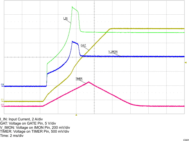 Figure 29. Inrush Mode at Hot-Swap Circuit Insertion
7.4.2 Inrush Operation
After TPS24720 initialization is complete (as described in the Board Plug-In section) and EN is active, GATE is enabled (VGATE starts increasing). When VGATE reaches the MOSFET M1 gate threshold, a current flows into the downstream bulk storage capacitors. When this current exceeds the limit set by the power-limit engine, the gate of the MOSFET is regulated by a feedback loop to make the MOSFET current rise in a controlled manner. This not only limits the capacitor-charging inrush current but it also limits the power dissipation of the MOSFET to safe levels. A more complete explanation of the power-limiting scheme is given in the section entitled Action of the Constant-Power Engine. When GATE is enabled, the TIMER pin begins to charge the timing capacitor CT with a current of approximately 10 µA. The TIMER pin continues to charge CT until V(GATE – VCC) reaches the timer activation voltage (5.9 V for VVCC = 12 V). The TIMER then begins to discharge CT with a current of approximately 10 µA. This indicates that the inrush mode is finished. If the TIMER exceeds its upper threshold of 1.35 V before V(GATE – VCC) reaches the timer activation voltage, the GATE pin is pulled to GND and the hot-swap circuit enters either latch mode or auto-retry mode, depending upon the status of the LATCH pin (see LATCH).
The power limit feature is disabled once the inrush operation is finished and the hotswap circuit becomes a circuit breaker. The TPS24720 turns off the MOSFET M1 after a fault timer period once the load exceeds the current limit threshold.
7.4.3 Action of the Constant-Power Engine
Figure 30 illustrates the operation of the constant-power engine during start-up. The circuit used to generate the waveforms of Figure 30 was programmed to a power limit of 29.3 W by means of the resistor connected between PROG and GND. At the moment current begins to flow through the MOSFET, a voltage of 12 V appears across it (input voltage VVCC = 12 V), and the constant-power engine therefore allows a current of 2.44 A (equal to 29.3 W divided by 12 V) to flow. This current increases in inverse ratio as the drain-to-source voltage diminishes, so as to maintain a constant dissipation of 29.3 W. The constant-power engine adjusts the current by altering the reference signal fed to the current limit amplifier. The lower part of Figure 31 shows the measured power dissipated within the MOSFET, labeled FET PWR, remaining substantially constant during this period of operation, which ends when the current through the MOSFET reaches the current limit ILIM. This behavior can be considered a form of foldback limiting, but unlike the standard linear form of foldback limiting, it allows the power device to operate near its maximum capability, thus reducing the start-up time and minimizing the size of the required MOSFET.
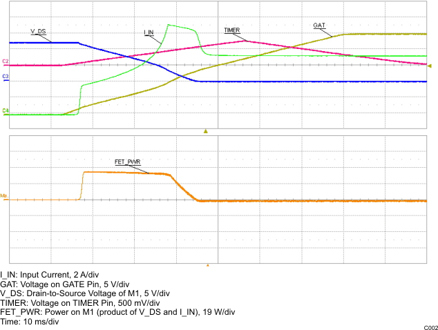 Figure 30. Computation of M1 Power Stress During Startup
7.4.4 Circuit Breaker and Fast Trip
The TPS24720 monitors load current by sensing the voltage across RSENSE. The TPS24720 incorporates two distinct thresholds: a current-limit threshold and a fast-trip threshold.
The functions of circuit breaker and fast-trip turn off are shown in Figure 31 through Figure 34.
Figure 31 shows the behavior of the TPS24720 when a fault in the output load causes the current passing through RSENSE to increase to a value above the current limit but less than the fast-trip threshold. When the current exceeds the current-limit threshold, a current of approximately 10 μA begins to charge timing capacitor CT. If the voltage on CT reaches 1.35 V, then the external MOSFET is turned off. The TPS24720 either latches off or commences a restart cycle, depending upon the state of the LATCH pin. In either event, fault pin FLTb pulls low to signal a fault condition. Overload between the current limit and the fast-trip threshold is permitted for this period. This shutdown scheme is sometimes called an electronic circuit breaker.
The fast-trip threshold protects the system against a severe overload or a dead short circuit. When the voltage across the sense resistor RSENSE exceeds the 60-mV fast-trip threshold, the GATE pin immediately pulls the external MOSFET gate to ground with approximately 1 A of current. This extremely rapid shutdown may generate disruptive transients in the system, in which case a low-value resistor inserted between the GATE pin and the MOSFET gate can be used to moderate the turn off current. The fast-trip circuit holds the MOSFET off for only a few microseconds, after which the TPS24720 turns back on slowly, allowing the current-limit feedback loop to take over the gate control of M1. Then the hot-swap circuit goes into latch mode or auto-retry mode, depending on pre-determined conditions. Figure 33 and Figure 34 illustrate the behavior of the system when the current exceeds the fast-trip threshold.
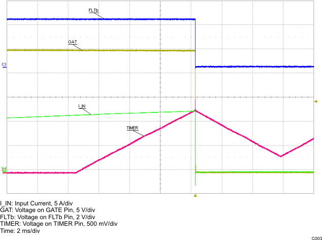 Figure 31. Circuit-Breaker Mode During Overload Condition
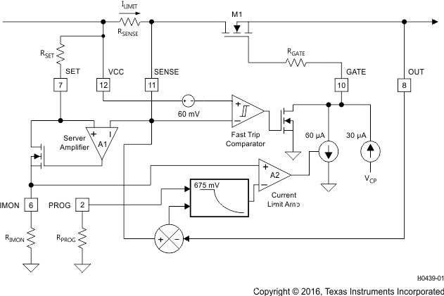 Figure 32. Partial Diagram of the TPS24720 With Selected External Components
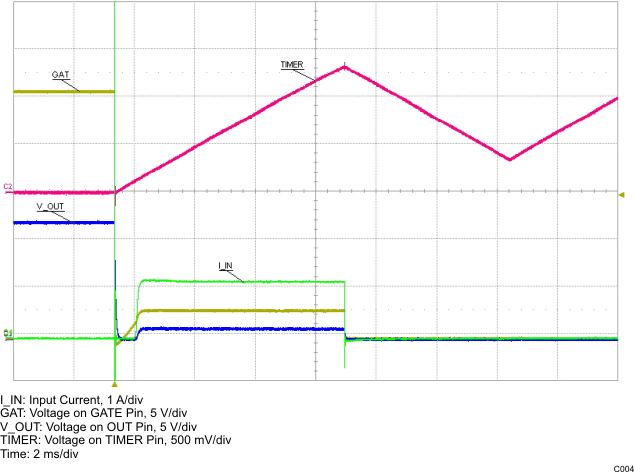 Figure 33. Current Limit During Output-Load Short-Circuit Condition (Overview)
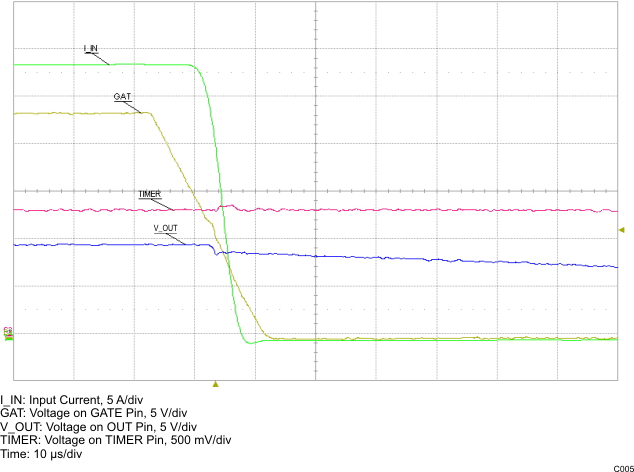 Figure 34. Current Limit During Output-Load Short-Circuit Condition (Onset)
7.4.5 Automatic Restart
If LATCH is connected to GND, then the TPS24720 automatically initiates a restart after a fault has caused it to turn off the external MOSFET M1. Internal control circuits use CT to count 16 cycles before re-enabling M1 as shown in Figure 35. This sequence repeats if the fault persists. The timer has a 1 : 1 charge-to-discharge current ratio. For the very first cycle, the TIMER pin starts from 0 V and rises to the upper threshold of 1.35 V and subsequently falls to 0.35 V before restarting. For the following 16 cycles, 0.35 V is used as the lower threshold. This small duty cycle often reduces the average short-circuit power dissipation to levels associated with normal operation and eliminates special thermal considerations for surviving a prolonged output short.
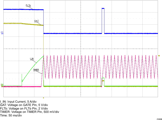 Figure 35. Auto-Restart Cycle Timing
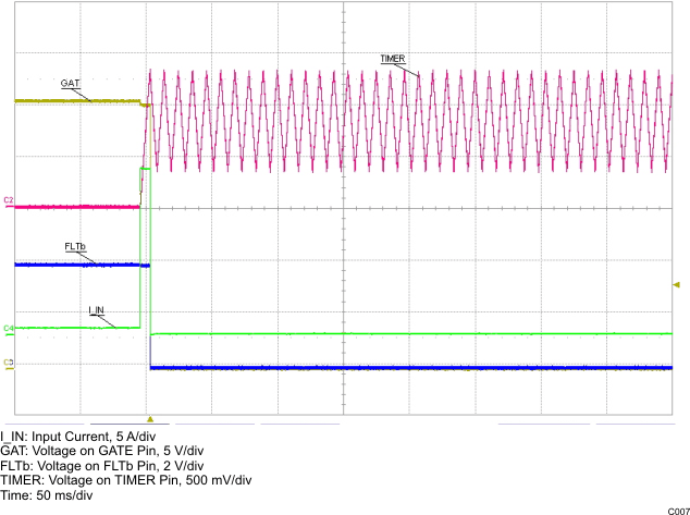 Figure 36. Latch After Overload Fault
7.4.6 PGb, FLTb, and Timer Operations
The open-drain PGb output provides a deglitched end-of-inrush indication based on the voltage across M1. PGb is useful for preventing a downstream dc/dc converter from starting while its input capacitor COUT is still charging. PGb goes active-low about 3.4 ms after COUT is charged. This delay allows M1 to fully turn on and any transients in the power circuits to end before the converter starts up. This type of sequencing prevents the downstream converter from demanding full current before the power-limiting engine allows the MOSFET to conduct the full current set by the current limit ILIM. Failure to observe this precaution may prevent the system from starting. The pullup resistor shown on the PGb pin in the typical application diagram on the front page is illustrative only; the actual connection to the converter depends on the application. The PGb pin may indicate that inrush has ended before the MOSFET is fully enhanced, but the downstream capacitor will have been charged to substantially its full operating voltage. Care should be taken to ensure that the MOSFET on-resistance is sufficiently small to ensure that the voltage drop across this transistor is less than the minimum power-good threshold of 140 mV. After the hot-swap circuit successfully starts up, the PGb pin can return to a high-impedance status whenever the drain-to-source voltage of MOSFET M1 exceeds its upper threshold of 340 mV, which presents the downstream converters a warning flag. This flag may occur as a result of overload fault, output short fault, input overvoltage, higher die temperature, or the GATE shutdown by UVLO, EN or ENSD.
FLTb is an indicator that the allowed fault-timer period during which the load current can exceed the programmed current limit (but not the fast-trip threshold) expires. The fault timer starts when a current of approximately 10 μA begins to flow into the external capacitor, CT, and ends when the voltage of CT reaches TIMER upper threshold, i.e., 1.35 V. FLTb pulls low at the end of the fault timer. Otherwise, FLTb assumes a high-impedance state.
The fault-timer state requires an external capacitor CT connected between the TIMER pin and GND pin. The duration of the fault timer is the charging time of CT from 0 V to its upper threshold of 1.35 V. The fault timer begins to count under any of the following three conditions:
- In the inrush mode, TIMER begins to source current to the timer capacitor, CT, when MOSFET M1 is enabled. TIMER begins to sink current from the timer capacitor, CT when V(GATE – VCC) exceeds the timer activation voltage (see the Inrush Operation section). If V(GATE – VCC) does not reach the timer activation voltage before TIMER reaches 1.35 V, then the TPS24720 disables the external MOSFET M1. After the MOSFET turns off, the timer goes into either latch mode or retry mode, depending on the LATCH pin status.
- In an overload fault, TIMER begins to source current to the timer capacitor, CT, when the load current exceeds the programmed current limits. When the timer capacitor voltage reaches its upper threshold of 1.35 V, TIMER begins to sink current from the timer capacitor, CT, and the GATE pin is pulled to ground. After the fault timer period, TIMER may go into latch mode or retry mode, depending on the LATCH pin status.
- In output short-circuit fault, TIMER begins to source current to the timer capacitor, CT, when the load current exceeds the programmed current limits following a fast-trip shutdown of M1. When the timer capacitor voltage reaches its upper threshold of 1.35 V, TIMER begins to sink current from the timer capacitor, CT, and the GATE pin is pulled to ground. After the fault timer period, TIMER may go into latch mode or retry mode, depending on the LATCH pin status.
If the fault current drops below the programmed current limit within the fault timer period, VTIMER decreases and the pass MOSFET remains enabled.
The behaviors of TIMER are different in the latch mode and retry mode. If the timer capacitor reaches the upper threshold of 1.35 V, then:
- In latch mode, the TIMER pin continues to charge and discharge the attached capacitor periodically until TPS24720 is disabled by UVLO, EN, ENSD, or OV, as shown in Figure 36.
- In retry mode, TIMER charges and discharges CT between the lower threshold of 0.35 V and the upper threshold of 1.35 V for sixteen cycles before the TPS24720 attempts to re-start. The TIMER pin is pulled to GND at the end of the 16th cycle of charging and discharging and then ramps from 0 V to 1.35 V for the initial half-cycle in which the GATE pin sources current. This periodic pattern is stopped once the overload fault is removed or the TPS24720 is disabled by UVLO, EN, ENSD, or OV.
7.4.7 Overtemperature Shutdown
The TPS24720 includes a built-in overtemperature shutdown circuit designed to disable the gate driver if the die temperature exceeds approximately 140°C. An overtemperature condition also causes the FLTb, FFLTb and PGb pins to go to high-impedance states. Normal operation resumes once the die temperature has fallen approximately 10°C.
7.4.8 Start-Up of Hot-Swap Circuit by VCC or EN
The connection and disconnection between a load and the input power bus are controlled by turning on and turning off the MOSFET, M1.
The TPS24720 has two ways to turn on MOSFET M1:
- Increasing VVCC above UVLO upper threshold while EN is already higher than its upper threshold sources current to the GATE pin. After an inrush period, the TPS24720 fully turns on MOSFET M1.
- Increasing EN above its upper threshold while VVCC is already higher than the UVLO upper threshold sources current to the GATE pin. After an inrush period, the TPS24720 fully turns on MOSFET M1.
The EN pin can be used to start up the TPS24720 at a selected input voltage VVCC.
To isolate the load from the input power bus, the GATE pin sinks current and pulls the gate of MOSFET M1 low. The MOSFET can be disabled by any of the following conditions: UVLO, EN, ENSD, load current above the current-limit threshold, hard short at load, OV, or OTSD. Three separate mechanisms pull down the GATE pin:
- GATE is pulled down by an 11-mA current source when any of the following occurs.
- The fault timer expires during an overload current fault (VIMON > 675 mV).
- VEN is below its falling threshold.
- VVCC drops below the UVLO threshold.
- VOV is above its rising threshold.
- GATE is pulled down by a 1-A current source for 13.5 μs when a hard output short circuit occurs and V(VCC – SENSE) is greater than 60 mV, i.e., the fast-trip shutdown threshold. After fast-trip shutdown is complete, an 11-mA sustaining current ensures that the external MOSFET remains off.
- GATE is discharged by a 20-kΩ resistor to GND if the chip die temperature exceeds the OTSD rising threshold or ENSD is pulled low.
7.4.9 Minimization of Power Dissipation at STANDY by ENSD
The ENSD pin enables the use of TPS24720 in applications requiring a low-power standby mode. When this pin is pulled below its threshold voltage, all the internal circuitry is switched off and the GATE pin is discharged to GND through a 20-kΩ resistor. Thus, the MOSFET is disabled and power consumption is kept to a minimum. The correct procedure to go into standby mode is first to shut down the TPS24720 by using the EN pin and then to pull the ENSD pin low.
7.4.10 Fault Detection of MOSFET Short With FFLTb
One of the salient features of the TPS24720 is the detection of short-circuited MOSFETs by the FFLTb pin. The FFLTb is pulled low to indicate a FET short if all the following conditions occur.
- EN is below its threshold voltage.
- VVCC is above the UVLO threshold.
- VIMON > 103 mV.
The fact that GATE is turned off but current is still flowing through RSENSE indicates a drain-to-source short.
