SLVSBY8D May   2013  – June 2020 TPS2513 , TPS2513A , TPS2514 , TPS2514A

PRODUCTION DATA.  

  1. Features
  2. Applications
  3. Description
    1.     Device Images
      1.      Simplified Schematic
  4. Revision History
  5. Device Options
  6. Pin Configuration and Functions
    1.     Pin Functions: TPS2513x
    2.     Pin Functions: TPS2514x
  7. Specifications
    1. 7.1 Absolute Maximum Ratings
    2. 7.2 ESD Ratings
    3. 7.3 Recommended Operating Conditions
    4. 7.4 Thermal Information
    5. 7.5 Electrical Characteristics
    6. 7.6 Typical Characteristics
  8. Detailed Description
    1. 8.1 Overview
    2. 8.2 Functional Block Diagrams
    3. 8.3 Feature Description
      1. 8.3.1 Dedicated Charging Port (DCP)
      2. 8.3.2 Short the D+ Line to the D– Line
      3. 8.3.3 Divider DCP
      4. 8.3.4 Applying 1.2 V to the D+ Line and 1.2 V to the D– Line
      5. 8.3.5 DCP Auto-Detect
      6. 8.3.6 Undervoltage Lockout (UVLO)
    4. 8.4 Device Functional Modes
  9. Applications and Implementation
    1. 9.1 Application Information
    2. 9.2 Typical Applications
      1. 9.2.1 Design Requirements
      2. 9.2.2 Detailed Design Procedure
        1. 9.2.2.1 Divide Mode Selection of 5-W and 10-W USB Chargers
      3. 9.2.3 Application Curves
  10. 10Power Supply Recommendations
  11. 11Layout
    1. 11.1 Layout Guidelines
    2. 11.2 Layout Example
  12. 12Device and Documentation Support
    1. 12.1 Related Links
    2. 12.2 Receiving Notification of Documentation Updates
    3. 12.3 Support Resources
    4. 12.4 Trademarks
    5. 12.5 Electrostatic Discharge Caution
    6. 12.6 Glossary
  13. 13Mechanical, Packaging, and Orderable Information

Package Options

Mechanical Data (Package|Pins)
Thermal pad, mechanical data (Package|Pins)
Orderable Information

Typical Characteristics

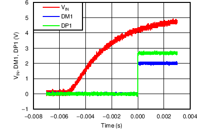
TPS2513 TPS2513A TPS2514 TPS2514A C001_SLVSBY8.png
Figure 1. Power On (DM1 and DP1)
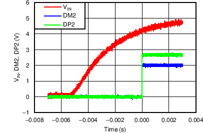
TPS2513 TPS2513A TPS2514 TPS2514A C003_SLVSBY8.png
Figure 3. Power On (DM2 and DP2)
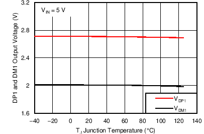
TPS2513 TPS2513A TPS2514 TPS2514A C005_SLVSBY8.png
Figure 5. DP1 and DM1 Output Voltage vs Temperature
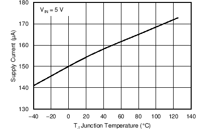
TPS2513 TPS2513A TPS2514 TPS2514A C007_SLVSBY8.png
Figure 7. Supply Current vs Temperature
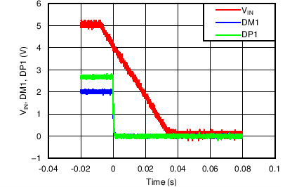
TPS2513 TPS2513A TPS2514 TPS2514A C002_SLVSBY8.png
Figure 2. Power Off (DM1 and DP1)
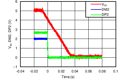
TPS2513 TPS2513A TPS2514 TPS2514A C004_SLVSBY8.png
Figure 4. Power Off (DM2 and DP2)
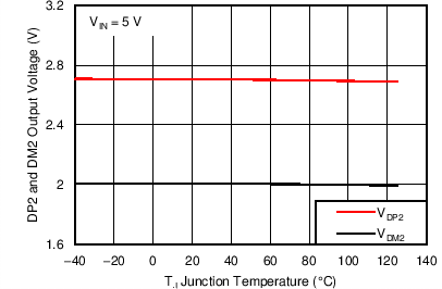
TPS2513 TPS2513A TPS2514 TPS2514A C006_SLVSBY8.png
Figure 6. DP2 and DM2 Output Voltage vs Temperature